
NUC-310 · Lesson 4 of 12 · 19 min
Semiconductor detectors
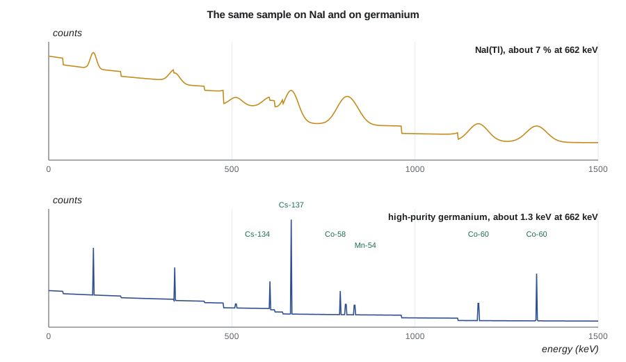
The counting room's most valuable instruments sit in thick lead shields at the back of the lab, each with a copper cold finger running down into a dewar or an electric cooler. They are high-purity germanium (HPGe) detectors, and Marcel calls them the station's fingerprint readers. A NaI spectrum of a reactor coolant sample shows a few broad lumps. A germanium spectrum of the same sample shows dozens of sharp peaks, each the signature of a single radionuclide. This lesson explains why.
Semiconductors as solid ion chambers
A semiconductor detector works like an ion chamber made of solid material. In a crystal such as silicon or germanium, electrons are bound in a filled valence band, separated by a small band gap from an empty conduction band. Radiation depositing energy lifts electrons across the gap, leaving positive holes. An electric field sweeps electrons and holes to opposite electrodes, and the collected charge is proportional to the energy deposited.
The key advantage over a gas or a scintillator is the small energy needed per charge carrier. Creating one electron-hole pair takes about 2.96 eV in germanium at its operating temperature and about 3.6 eV in silicon, compared with about 30 eV per ion pair in a gas and roughly 100 eV or more per photoelectron in a NaI scintillator once light-collection losses are counted. Ten times more carriers per unit energy means far smaller statistical fluctuations and much better energy resolution.
Junctions and depletion
A plain block of semiconductor would conduct too much current to detect the tiny signal of a single event. Detectors are therefore built as reverse-biased diodes. At a junction between p-type and n-type material, carriers diffuse across and leave a region with no free carriers, called the depletion region. Applying a reverse bias widens it. Only within the depleted volume is the field present and the leakage current small, so the depleted volume is the sensitive volume of the detector.
The depletion depth \(d\) grows with the square root of the bias voltage \(V\) and falls with the net impurity concentration \(N\):
This is why germanium for gamma spectroscopy has to be extraordinarily pure. To deplete several centimeters with a few thousand volts, the net impurity concentration must be around \(10^{10}\) atoms per cubic centimeter, about one impurity atom per \(10^{12}\) germanium atoms. Zone refining of germanium to that purity, developed in the 1970s, made large HPGe detectors practical and largely replaced the earlier lithium-drifted germanium detectors, which had to be kept cold at all times.
# Semiconductor detectors: carriers, Fano-limited resolution and depletion depth.
import math
w_ge, F = 2.96, 0.08          # eV per electron-hole pair and Fano factor for germanium (approx.)
noise_keV = 0.7               # electronic noise FWHM, keV (illustrative)
for E in (122, 662, 1332):     # keV
    N = E * 1000 / w_ge
    stat = 2.355 * math.sqrt(F * w_ge * E * 1000) / 1000    # keV FWHM
    tot = math.sqrt(stat**2 + noise_keV**2)
    print(f"{E:5d} keV: {N:8.0f} pairs, Fano FWHM {stat:4.2f} keV, with noise {tot:4.2f} keV ({100*tot/E:5.2f} %)")

# Compare with NaI at 662 keV (about 7 %)
print(f"NaI at 662 keV: about {0.07*662:4.0f} keV FWHM")

# Depletion depth of a reverse-biased junction: d = sqrt(2 eps V / (q N))
eps = 16 * 8.854e-12; q = 1.602e-19
N = 1e16                    # net impurity per m3 (high-purity germanium, approx.)
for Vb in (500, 2000, 4000):
    d = math.sqrt(2 * eps * Vb / (q * N))
print(f"bias {Vb:4d} V: depletion depth {100*d:5.2f} cm")122 keV: 41216 pairs, Fano FWHM 0.40 keV, with noise 0.81 keV ( 0.66 %) 662 keV: 223649 pairs, Fano FWHM 0.93 keV, with noise 1.17 keV ( 0.18 %) 1332 keV: 450000 pairs, Fano FWHM 1.32 keV, with noise 1.50 keV ( 0.11 %) NaI at 662 keV: about 46 keV FWHM bias 500 V: depletion depth 0.94 cm bias 2000 V: depletion depth 1.88 cm bias 4000 V: depletion depth 2.66 cm
Energy resolution and the Fano factor
If each event's carriers were produced independently, their number \(N = E/w\) would fluctuate with standard deviation \(\sqrt{N}\), as in a Poisson process. In reality, energy sharing between ionization and lattice vibrations is correlated, and the variance is smaller by the Fano factor \(F\), about 0.06 to 0.1 for germanium. The statistical contribution to the FWHM in energy units is
Electronic noise from the detector's leakage current and capacitance and from the preamplifier adds in quadrature, along with a term from incomplete charge collection. The program shows that the statistical width at 662 keV is under 1 keV, and adding typical electronic noise gives about 1.2 keV, or 0.18 %. Good coaxial HPGe detectors are specified at about 1.8 to 2.0 keV FWHM at 1332 keV, against roughly 60 keV for a NaI crystal at the same energy, a factor of thirty better.
Why germanium is cooled
Germanium's small band gap of about 0.67 eV is what gives it so many carriers per unit energy, but it also lets thermal energy excite electrons across the gap at room temperature. The leakage current would swamp the signal. HPGe detectors are therefore operated at about 77 K, the boiling point of liquid nitrogen, or at similar temperatures using electric mechanical coolers. HPGe crystals can be warmed up when not in use, but the bias must be removed first. A detector biased while warm can draw damaging current.
Mechanical coolers avoid weekly liquid nitrogen fills and allow portable HPGe systems for field measurements, such as in situ gamma spectrometry of soil, but they add vibration, which can broaden peaks through microphonic noise unless isolated. Many counting rooms now use them for their convenience and safety, since liquid nitrogen brings oxygen-deficiency and cold-burn hazards of its own.
Detector geometries
HPGe crystals are made in several shapes. A closed-end coaxial detector is a cylinder with a central hole bored from the back, which gives a large sensitive volume for high-energy gamma rays and is the usual choice for general environmental and effluent work. Its efficiency is quoted relative to a 3 inch by 3 inch NaI crystal for 1332 keV photons at 25 cm, so a 40 % relative efficiency detector has 40 % of that NaI's peak efficiency. Planar detectors are thin discs with thin entrance windows, used for X-rays and low-energy gamma rays. Broad-energy detectors combine a thin front contact with a reasonable thickness, covering roughly 3 keV to 3 MeV. Well detectors have a hole into which a small sample is placed, giving nearly \(4\pi\) geometry and very high efficiency for small samples.
The type of semiconductor affects which surface is thin. In p-type coaxial detectors the outer contact is a lithium-diffused layer several hundred micrometers thick, which absorbs low-energy photons. In n-type detectors the outer contact is a much thinner implanted layer, so they see lower energies and are also more resistant to fast-neutron damage, a useful property near reactor systems.
Silicon detectors
Silicon has too low an atomic number and density to be efficient for gamma rays above about 30 keV, but it is excellent for charged particles and low-energy X-rays and works at or near room temperature. Passivated implanted planar silicon (PIPS) detectors, thin discs with a very thin entrance window, are the standard detectors for alpha spectrometry. In a vacuum chamber they resolve alpha peaks about 20 keV wide, enough to separate the alpha emitters found in bioassay samples and in decommissioning surveys. Silicon drift detectors measure X-rays with good resolution using small Peltier coolers, and silicon diodes are the sensing element in many electronic personal dosimeters.
Room-temperature compound semiconductors
For field instruments that cannot carry a cooler, compound semiconductors with larger band gaps and higher atomic numbers are used. Cadmium zinc telluride (CZT) operates at room temperature, stops gamma rays reasonably well and achieves resolutions of a few percent or better at 662 keV, between NaI and HPGe. CZT crystals are small and expensive, and charge trapping, especially of holes, complicates their response, but they are now common in compact radionuclide identifiers and in some area monitors.
| Detector | Energy per carrier | Typical FWHM at 662 keV | Operating temperature | Main use |
|---|---|---|---|---|
| NaI(Tl) scintillator | about 100 eV per photoelectron or more | about 46 keV (7 %) | Room | Screening, high efficiency |
| CZT | about 4.6 eV | about 10–15 keV (1.5–2 %) | Room | Hand-held identification |
| HPGe coaxial | 2.96 eV | about 1.2–1.5 keV (0.2 %) | about 77 K | Laboratory gamma spectrometry |
| Silicon (PIPS) | 3.6 eV | not used for gamma rays | Room | Alpha spectrometry, X-rays |
Charge collection and pulse shape
In a large coaxial HPGe crystal, electrons and holes may have to travel several centimeters to the electrodes. Their drift velocities near saturation are about \(10^{7}\) cm/s, so collection takes a few hundred nanoseconds, and the exact time depends on where in the crystal the interaction happened. The preamplifier output therefore rises over a variable time. Spectroscopy amplifiers use shaping times of a few microseconds, long compared with the collection time, so that every event's full charge is measured regardless of where it occurred. Shorter shaping handles higher count rates but loses resolution through ballistic deficit, the incomplete integration of slowly collected charge. Lesson 7 returns to these trade-offs.
The shape of the rising edge also carries information. Analyzing it can show whether an event deposited its energy in one place or in several, which distinguishes photoelectric events from multiple Compton scatters. Research detectors use this to reject background, and segmented germanium arrays use it to locate interactions in three dimensions. For routine laboratory work the main practical consequence is simpler: count rate, shaping time and resolution are linked, and a detector set up for a hot reactor coolant sample is not set up optimally for an environmental sample.
Efficiency, size and cost
Germanium is less efficient than NaI for the same size, because its atomic number (32) is lower than that of iodine (53), and large HPGe crystals are costly to grow. A laboratory therefore chooses detector size for its work. An environmental laboratory measuring trace cesium-137 in soil and food wants a large, low-background coaxial detector, often 50 to 100 % relative efficiency, and long counting times of a day or more. A station laboratory counting reactor coolant, filters and waste samples deals with much higher activities and may prefer a smaller detector placed further from the sample to keep dead time and pile-up low. Both need careful efficiency calibration for every sample geometry they use, because peak efficiency depends on energy, distance, container shape, fill height and sample density. Lesson 11 shows how that calibration is built and checked.
Coincidence summing is one effect that becomes larger as efficiency rises. Nuclides such as cobalt-60 emit two gamma rays in cascade, almost simultaneously. If both are detected, the detector records one event with the summed energy, and both individual peaks lose counts. In a well detector or with a sample placed on the end cap, the loss can be ten percent or more and must be corrected; at larger distances it becomes small.
Radiation damage and care
Semiconductor detectors are damaged by fast neutrons and heavy charged particles, which displace atoms from the lattice and create traps for charge carriers. Trapping causes peaks to develop low-energy tails and broaden. In a counting room this is rarely a concern, but detectors used near reactor systems or for in situ work in high fields degrade over time. Damaged HPGe crystals can often be restored by an annealing cycle at elevated temperature, performed by the manufacturer or a trained technician.
Germanium detectors are also expensive, and most damage comes from handling. Marcel's laboratory rules are short: never bias a warm detector, never touch the end cap, ramp high voltage slowly, keep the shield closed when not in use, and record every warm-up in the detector log. The log matters because changes in resolution or efficiency are the first sign of trouble, and a quality control program (lesson 11) compares daily check-source results against limits set from that history.
At TVA plants, HPGe results feed effluent reports and the radiological environmental monitoring program, so laboratories maintain documented calibrations and participate in interlaboratory comparison programs.
Hana's lesson from the fingerprint readers
Hana's notes end with a sentence she later uses when training new technicians. Germanium gives about ten times more carriers per unit energy than a scintillator gives photoelectrons, and its Fano factor makes their fluctuation smaller still, so its peaks are thirty times narrower. The price is cooling, cost, care and lower efficiency per unit volume. When the question is how much gamma activity is present, NaI is often enough. When the question is exactly which radionuclides are present, nothing replaces germanium.
Summary and key terms
- Semiconductor detectors collect electron-hole pairs in a depleted, reverse-biased crystal.
- Germanium needs about 2.96 eV per pair, giving many carriers and excellent resolution.
- Depletion depth grows as √(V/N); high-purity germanium makes thick sensitive volumes possible.
- The Fano factor reduces statistical fluctuation; HPGe resolution is about 0.2 % at 662 keV.
- Germanium must be cooled to about 77 K to suppress thermal leakage current.
- Silicon detectors serve alpha spectrometry and X-rays; CZT gives room-temperature spectroscopy.
- Band gap
- The energy separating the valence and conduction bands of a semiconductor.
- Depletion region
- The carrier-free zone of a reverse-biased junction that forms the sensitive volume.
- Fano factor
- The ratio of the observed variance in carrier number to the Poisson variance.
- High-purity germanium
- Germanium refined to about 10¹⁰ impurities per cm³ for thick depletion.
- Relative efficiency
- HPGe peak efficiency at 1332 keV relative to a 3 by 3 inch NaI crystal at 25 cm.
- Charge trapping
- Capture of carriers at defects, which broadens and tails spectral peaks.
Practice problems
Work each problem on paper first, then reveal the answer to check.
How many electron-hole pairs does a 1000 keV photon make in germanium?
Show answer
10⁶/2.96 ≈ 3.4 × 10⁵.
Using F = 0.08 and w = 2.96 eV, find the statistical FWHM at 1000 keV.
Show answer
2.355√(0.08 × 2.96 × 10⁶) eV ≈ 1.15 keV.
If depletion depth is 1 cm at 500 V, what voltage gives 2 cm?
Show answer
Depth ∝ √V, so 4 × 500 = 2000 V.
Why must the bias be removed before an HPGe detector warms up?
Show answer
Leakage current at high temperature can damage the detector and preamplifier.
Why is silicon not used for high-energy gamma rays?
Show answer
Its low density and atomic number give low gamma efficiency.
What does a low-energy tail on HPGe peaks suggest?
Show answer
Charge trapping, possibly from neutron damage.
Lesson quiz · 5 questions
Score 60% or more to complete this lesson.
Create a free account to save your progress, take quizzes and earn a certificate.