
ELE-470 · Lesson 1 of 12 · 29 min
Power semiconductor devices
Power electronics is the technology of converting electrical energy from one form to another using semiconductor switches: AC to DC in rectifiers and power supplies, DC to DC at different voltages, DC to AC in inverters, and AC at one frequency to AC at another in motor drives. Almost all electrical energy now passes through a power electronic converter at some point between generation and use: in solar inverters, wind turbine converters, HVDC links, battery chargers, electric vehicles, LED drivers, every computer power supply and the uninterruptible power supplies and server power shelves of data centres. The central idea is simple: a switch that is fully on has almost no voltage across it, and a switch that is fully off carries almost no current, so in either state it dissipates very little power. By switching rapidly between these states and filtering the result with inductors and capacitors, converters can control power with efficiencies of 95% to over 99%. This course covers devices (this lesson), thermal design, rectifiers, magnetics, DC-DC converters and their control, inverters, EMI, motor drives, renewable and storage converters, and HVDC, ending with a design project; the section at the end of this lesson shows how the twelve lessons fit together.
Why switching, not resistance
A linear regulator controls power by dropping excess voltage across a transistor operating as a variable resistor, wasting the difference as heat. Dropping 48 V to 12 V at 10 A this way would waste 360 W to deliver 120 W, an efficiency of 25%. A switching converter instead chops the input into pulses and averages them with an inductor: at a duty cycle of 25%, the average is 12 V, and the only losses are the small conduction and switching losses of the devices and the losses in the magnetic components. The trade-offs are complexity, electromagnetic interference from fast switching, and ripple that must be filtered.
The ideal switch and real devices
An ideal switch has zero voltage when on, zero current when off, switches instantly and needs no control power. Real devices fall short in four ways: on-state voltage drop or resistance (conduction loss), finite switching times during which voltage and current overlap (switching loss), limited voltage and current ratings, and the need for gate drive circuits. Devices are also distinguished by whether they can be turned on and off by a control signal, and by whether they block voltage and conduct current in one or both directions.
| Device | Control | Typical ratings | Typical switching frequency | Main uses |
|---|---|---|---|---|
| Diode | None (turns on when forward biased) | Up to kV and kA | Line frequency to MHz (fast types) | Rectifiers, freewheeling paths |
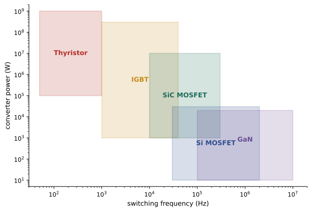
| Thyristor (SCR) | Gate turns on; turns off when current falls to zero | Up to about 10 kV, several kA | Line frequency | Controlled rectifiers, HVDC, soft starters |
| Power MOSFET (Si) | Voltage-controlled on and off | Up to about 900 V; best below 200 V | 50 kHz to over 1 MHz | Low-voltage DC-DC, server power, chargers |
| IGBT | Voltage-controlled on and off | 600 V to 6.5 kV, up to kA | 2 to 30 kHz | Motor drives, UPS, traction, wind and solar |
| SiC MOSFET | Voltage-controlled on and off | 650 V to 3.3 kV | 20 to 200 kHz | EV inverters, solar, fast chargers, high-efficiency UPS |
| GaN HEMT | Voltage-controlled on and off | Up to about 650 V | 100 kHz to several MHz | Compact adapters, server and telecom power |
Diodes
A power diode conducts when its anode is more positive than its cathode by about 0.7 V to 1.5 V (higher for high-voltage devices) and blocks reverse voltage otherwise. When a conducting diode is suddenly reverse biased, stored charge must be removed before it blocks, causing a brief reverse recovery current that adds to switching losses in the opposing switch and generates electromagnetic noise. Fast-recovery and soft-recovery diodes reduce this, and Schottky diodes (metal-semiconductor junctions) have very low forward drop and almost no recovery charge but low voltage ratings in silicon. Silicon carbide Schottky diodes combine high voltage ratings with negligible recovery and are widely used in power factor correction stages.
Thyristors
A thyristor, or silicon-controlled rectifier (SCR), is a four-layer device that blocks in both directions until a gate pulse turns it on; it then latches on and stays on until its current falls below a holding level, which in AC circuits happens naturally at the current zero. Thyristors have very high voltage and current ratings and robust surge capability, so they remain the device of choice for line-frequency controlled rectifiers, soft starters for large motors, static VAR compensators and classic HVDC converters. Their main limitation is that they cannot be turned off by the gate, which restricts them to circuits with natural commutation.
MOSFETs
A power MOSFET is turned on by applying a gate-source voltage (typically 10 V to 15 V for silicon devices) that charges the gate capacitance and creates a conducting channel. When on, it behaves like a resistance \(R_{DS(on)}\), so conduction loss is \(I^2 R_{DS(on)}\). It switches very quickly because it has no stored minority charge, and it conducts in both directions when on, which allows synchronous rectification (replacing diodes with MOSFETs to cut losses at low voltage). Its weaknesses are that \(R_{DS(on)}\) rises steeply with voltage rating in silicon, and that \(R_{DS(on)}\) increases by roughly 50% to 100% from 25 °C to 125 °C, which must be included in loss estimates. Silicon MOSFETs dominate low-voltage, high-frequency converters such as the 48 V and 12 V stages in server power.
IGBTs
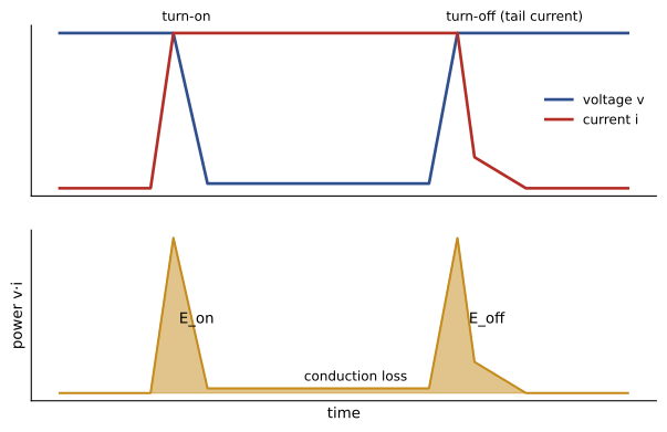
The insulated-gate bipolar transistor (IGBT) combines a MOSFET input with a bipolar output structure. It is controlled by gate voltage like a MOSFET but, when on, injects minority carriers that reduce its on-state resistance, so it has a nearly constant on-state voltage \(V_{CE(sat)}\) of about 1.5 V to 3 V even at high voltage ratings. The stored charge slows turn-off, producing a tail current that causes significant switching loss, which limits practical switching frequencies to tens of kilohertz. IGBTs are the workhorse of medium- and high-power converters: industrial motor drives, UPS inverters, solar and wind converters, and traction drives. They are packaged as modules containing several IGBTs with anti-parallel diodes, or as press-pack devices for the highest powers.
Wide-bandgap devices: SiC and GaN
Silicon carbide (SiC) and gallium nitride (GaN) are wide-bandgap semiconductors: their bandgap is about three times that of silicon, giving a critical electric field roughly ten times higher. This allows much thinner drift regions for the same voltage rating, and therefore much lower on-resistance and capacitance. The results are higher efficiency, higher switching frequencies (allowing smaller inductors, capacitors and transformers), and higher temperature capability. SiC MOSFETs have displaced silicon IGBTs in many electric vehicle inverters, fast chargers, solar inverters and high-efficiency UPS systems; GaN transistors power compact laptop adapters and are increasingly used in high-density server power supplies. Their higher cost per die is falling, and their very fast switching edges (tens of kilovolts per microsecond) create new challenges for gate drive design, electromagnetic interference and motor insulation (Lesson 9).
Conduction and switching losses
Device losses have two parts. Conduction loss occurs while the device carries current: for a MOSFET \(P = D\, I^2 R_{DS(on)}\) and for an IGBT approximately \(P = D\, V_{CE(sat)}\, I\), where \(D\) is the fraction of time the device conducts. Switching loss occurs during each transition, when voltage and current overlap; manufacturers give turn-on and turn-off energies \(E_{on}\) and \(E_{off}\) measured at specified conditions, and switching loss is approximately:
scaled linearly with voltage and current from the datasheet conditions. Switching loss grows with switching frequency, which is the fundamental trade-off of power electronics: higher frequency allows smaller filters and faster control, but costs efficiency.
import numpy as np

V, I = 800, 50
devices = {
    "Si IGBT": {"vce": 1.6, "ron": 0.0, "eon": 4.0e-3, "eoff": 3.5e-3, "rth": 0.30},
    "SiC MOSFET": {"vce": 0.0, "ron": 0.025, "eon": 0.9e-3, "eoff": 0.4e-3, "rth": 0.35},
}
duty, t_amb, rth_sink = 0.5, 40, 0.15
for name, d in devices.items():
    p_cond = duty * (d["vce"] * I + d["ron"] * I ** 2)
    print(name)
    for f in [5e3, 20e3, 50e3]:
        p_sw = (d["eon"] + d["eoff"]) * f
        total = p_cond + p_sw
        tj = t_amb + total * (d["rth"] + rth_sink)
print(f" f = {f / 1e3:4.0f} kHz conduction {p_cond:5.1f} W switching {p_sw:6.1f} W total {total:6.1f} W Tj = {tj:5.0f} C")Si IGBT f = 5 kHz conduction 40.0 W switching 37.5 W total 77.5 W Tj = 75 C f = 20 kHz conduction 40.0 W switching 150.0 W total 190.0 W Tj = 125 C f = 50 kHz conduction 40.0 W switching 375.0 W total 415.0 W Tj = 227 C SiC MOSFET f = 5 kHz conduction 31.2 W switching 6.5 W total 37.8 W Tj = 59 C f = 20 kHz conduction 31.2 W switching 26.0 W total 57.2 W Tj = 69 C f = 50 kHz conduction 31.2 W switching 65.0 W total 96.2 W Tj = 88 C
The comparison shows why SiC has spread rapidly. At 5 kHz both devices are acceptable; at 20 kHz the IGBT's switching losses dominate and its junction approaches its limit, while the SiC device runs cool; at 50 kHz the IGBT would fail. In practice designers choose the switching frequency to balance device losses against the size and cost of the magnetic components.
Thermal design
All device losses become heat that must flow from the semiconductor junction through the package, a thermal interface material and a heat sink to the air or a coolant. Thermal resistance \(R_{\theta}\) (in °C/W or K/W) relates temperature rise to power, just as electrical resistance relates voltage to current:
Junction temperatures are typically kept below 125 °C to 150 °C for silicon (higher limits apply to some SiC devices), with margin for overloads. Temperature also drives reliability: repeated heating and cooling (thermal cycling) fatigues bond wires and solder layers, so drives for applications with frequent load changes, such as elevators and traction, are sized for lower temperature swings.
Worked problem
Heat sink selection
An IGBT module dissipates 300 W. Its junction-to-case thermal resistance is 0.08 °C/W and case-to-sink is 0.03 °C/W. With an ambient of 45 °C and a maximum junction temperature of 125 °C, what heat sink thermal resistance is required?
Show solution
- Allowed rise: \(125 - 45 = 80\) °C.
- Total thermal resistance allowed: \(80/300 = 0.267\) °C/W.
- Heat sink: \(0.267 - 0.08 - 0.03 = 0.157\) °C/W.
Answer: A heat sink of no more than about 0.157 °C/W, which for 300 W typically requires forced air cooling or a liquid-cooled cold plate. Designers add margin for dust, fan failure and altitude, where thinner air reduces cooling.
Gate drives and protection
MOSFETs, IGBTs and wide-bandgap devices are controlled by gate drivers that charge and discharge the gate capacitance quickly with defined voltages (for example +15 V on and −5 V to −8 V off for many IGBT and SiC devices, so that noise cannot turn them on accidentally). In bridge circuits, the upper device's gate driver floats at the switching node voltage, so isolated drivers or bootstrap supplies are used. A dead time of hundreds of nanoseconds to a few microseconds between turning one device off and the other on prevents both switches in a leg from conducting at once (shoot-through), which would short the DC supply.
Protection is essential because semiconductors fail in microseconds:
- Desaturation (short-circuit) detection turns off an IGBT within a few microseconds if its voltage rises while on, indicating a short circuit.
- Snubber circuits and careful layout limit voltage overshoot caused by stray inductance during fast turn-off, since \(v = L\, di/dt\).
- Overcurrent, overvoltage and overtemperature monitoring shut the converter down safely.
- Semiconductor fuses rated for very fast clearing protect against internal faults.
Worked problem
Overshoot from stray inductance
A SiC MOSFET turns off 100 A in 50 ns. The commutation loop has 20 nH of stray inductance. What voltage overshoot occurs? How much would it be with an IGBT turning off the same current in 300 ns?
Show solution
- SiC: \(di/dt = 100/50 \times 10^{-9} = 2 \times 10^{9}\) A/s; \(v = 20 \times 10^{-9} \times 2 \times 10^9 = 40\) V.
- IGBT: \(di/dt = 3.33 \times 10^{8}\) A/s; \(v = 6.7\) V.
Answer: About 40 V for the SiC device versus about 7 V for the IGBT. Faster devices make layout critical: designers minimize loop inductance with laminated busbars, close-coupled capacitors and low-inductance modules, or slow the switching slightly at the cost of more loss.
Passive components
Every converter also contains inductors, transformers and capacitors, which are often larger and costlier than the semiconductors. Magnetic components store and transfer energy; their size falls as switching frequency rises, but core losses (from hysteresis and eddy currents) and winding losses (worsened at high frequency by the skin and proximity effects) rise. Capacitors filter ripple and supply pulsed currents; their ripple current rating and life, especially for electrolytic capacitors, whose life roughly halves for every 10 °C rise in temperature, frequently limit converter lifetime. Film capacitors last longer and are common in DC links of drives and inverters.
How this course is organized
The twelve lessons build from components to complete systems:
- Lesson 1 (this lesson): power semiconductor devices, losses and gate drives.
- Lesson 2: thermal design and reliability.
- Lesson 3: rectifiers, harmonics and power factor correction.
- Lesson 4: magnetics and capacitors.
- Lesson 5: DC-DC converters.
- Lesson 6: converter dynamics and control.
- Lesson 7: inverters, grid connection and UPS systems.
- Lesson 8: EMI, snubbers and layout.
- Lesson 9: motor drives.
- Lesson 10: power electronics for renewables, storage and electric vehicles.
- Lesson 11: high-power converters: HVDC and FACTS.
- Lesson 12: a converter design project.
Common mistakes
MistakeUsing a linear regulator for large voltage reductions at high current.
InsteadUse a switching converter; linear efficiency is limited to Vo/Vin.
MistakeEstimating MOSFET conduction loss with the 25 °C on-resistance.
InsteadUse the on-resistance at the expected junction temperature.
MistakeRaising switching frequency without checking switching loss.
InsteadCalculate (Eon + Eoff)·f and thermal limits.
MistakeIgnoring stray inductance with fast devices.
InsteadMinimize loop inductance; check L·di/dt overshoot.
MistakeOmitting dead time in a half-bridge.
InsteadInsert dead time to prevent shoot-through.
Summary and key terms
- Power electronics converts energy efficiently by switching devices fully on or off and filtering.
- Linear regulation wastes the voltage difference; switching converters reach 95% to over 99%.
- Diodes and thyristors suit rectification; MOSFETs, IGBTs, SiC and GaN are fully controllable.
- Wide-bandgap SiC and GaN allow higher voltage, frequency and efficiency.
- Losses are conduction plus switching, (Eon + Eoff)·f; frequency trades loss against filter size.
- Junction temperature = ambient + power × total thermal resistance.
- Gate drives, dead time, desaturation protection and low-inductance layout keep devices safe.
- Power electronics
- The conversion and control of electric power with semiconductor switches.
- Duty cycle
- The fraction of each switching period a switch is on.
- Reverse recovery
- The brief reverse current while a diode removes stored charge.
- Thyristor
- A latching device turned on by a gate pulse and off by current zero.
- IGBT
- A voltage-controlled bipolar device with low on-state voltage at high ratings.
- Wide-bandgap
- Semiconductors such as SiC and GaN with higher critical field than silicon.
- Switching loss
- Energy lost when voltage and current overlap during transitions.
- Thermal resistance
- Temperature rise per watt of heat flow.
- Dead time
- A delay preventing both switches in a leg from conducting together.
- Shoot-through
- Simultaneous conduction of both switches in a leg, shorting the supply.
Practice problems
Work each problem on paper first, then reveal the answer to check.
Efficiency of a linear regulator from 24 V to 5 V?
Show answer
5/24 ≈ 21%.
Which device cannot be turned off by its gate?
Show answer
The thyristor (SCR).
MOSFET with R_DS(on) = 8 mΩ at 125 °C carries 30 A at D = 0.6. Conduction loss?
Show answer
0.6 × 900 × 0.008 = 4.32 W.
IGBT: V_CE(sat) 1.8 V, 100 A, D = 0.5. Conduction loss?
Show answer
90 W.
Eon + Eoff = 6 mJ at 10 kHz. Switching loss?
Show answer
60 W.
Why do SiC devices allow higher switching frequency?
Show answer
Lower switching energies from thinner drift regions and no tail current.
150 W, R_θ total 0.4 °C/W, ambient 40 °C. Junction temperature?
Show answer
100 °C.
What is shoot-through and how is it prevented?
Show answer
Both leg switches on at once; prevented by dead time.
10 nH stray inductance, 60 A turned off in 20 ns. Overshoot?
Show answer
30 V.
How does temperature affect electrolytic capacitor life?
Show answer
Life roughly halves for each 10 °C rise.
Lesson quiz · 5 questions
Score 60% or more to complete this lesson.
Create a free account to save your progress, take quizzes and earn a certificate.