
ELE-445 · Lesson 9 of 12 · 23 min
Single-stage and differential amplifiers
With bias currents and a reference in hand, the CX-1 team turns to signal processing. The microphone preamplifier for the APS-2 must amplify a 10 mV signal from a pole-top microphone by up to about 30 dB without adding much noise, offset or hum. ELE-340 designed this front end from discrete parts. On the chip the same functions must be built from transistors sized one by one, under a power budget of a few tens of microamperes. This lesson designs the basic gain stages at the IC level, with active loads instead of resistors, and uses the gm/ID method to size the preamplifier's differential input stage for gain, bandwidth and offset.
The common-source stage with an active load
On a chip, resistors large enough to make good loads take enormous area and vary by twenty percent, so gain stages use transistors as loads. A common-source NMOS amplifier with a PMOS current-source load has a gain set by the input device's transconductance and the parallel output resistance of the two devices.
The second form shows the gm/ID view: the gain depends only on the input device's transconductance efficiency and the two devices' channel-length modulation, not on the bias current. Raising the current raises g_m and lowers r_o in proportion, leaving the gain unchanged; it raises only the bandwidth. With g_m/I_D = 15 V⁻¹ and both devices at L = 1 µm, so each λ is 0.04 V⁻¹, the gain is 15/0.08 ≈ 190. That is about 45 dB from one stage, and it explains why a two-stage op-amp, lesson 10's subject, easily reaches 80 dB.
The price of high gain is high output impedance, several megohms here, so the stage can drive only capacitive loads; and the output's quiescent level is set by the balance between two current sources, so it must be fixed by feedback, which is another reason that most IC gain stages live inside op-amps.
Followers and cascode gain stages
The common-drain stage, or source follower, has a gain slightly less than one, reduced further by the body effect when the device sits in the shared substrate, and an output resistance of about 1/g_m. It is the on-chip buffer for driving resistive loads and level shifting. It costs headroom, a V_GS from input to output, and it adds little noise.
The common-gate stage, with the input at the source, has a low input resistance of about 1/g_m and a non-inverting gain similar to the common-source stage. Its main use on chips is as the upper device of a cascode amplifier: a common-source input device with a common-gate device above it, loaded by a cascoded current source. Each cascode multiplies an output resistance by about g_m r_o, so the cascode amplifier's gain is roughly (g_m r_o)², several thousand. The telescopic and folded-cascode op-amps of lesson 10 are built from exactly this structure, at the cost of the headroom each stacked device consumes.
The differential pair at the IC level
Almost every precision analog input on a chip is differential, because a differential pair rejects common-mode noise, from the substrate, the supply and the cable, that a single-ended stage passes. The CX-1 preamplifier's input stage is a differential pair with a current-mirror load, the five-transistor stage that ELE-340 studied. The pair converts the input difference into a current difference; the mirror copies one side's current to the other, so the full differential current flows into the output node and the stage gives single-ended output with the gain of the full pair.
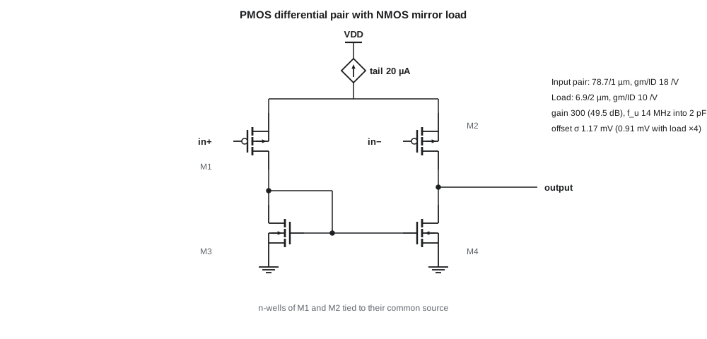
Priya chooses a PMOS input pair for three reasons. PMOS devices in this process have lower flicker noise than NMOS devices, which matters at audio frequencies where flicker noise dominates. Their n-wells can be tied to their common source, removing the body effect and isolating the pair from substrate noise that the digital half injects. And a PMOS pair can accept input common-mode voltages down to ground, which suits the microphone interface. The cost is that PMOS devices need about four times the width of NMOS devices for the same transconductance, which costs area and capacitance.
The gain of the mirror-loaded pair is g_m1 times the parallel combination of the output resistances of M2 and M4. Its common-mode rejection depends on the tail current source's output resistance and on matching: a common-mode input changes the tail current through the tail source's finite resistance, and any mismatch between the halves turns that change into an output. On a chip, where the tail is a cascoded current source of hundreds of megohms, the mismatch term usually dominates.
Sizing the CX-1 input stage
The stage must give a unity-gain frequency of at least 10 MHz into the 2 pF of the next stage, so that the closed-loop preamplifier has bandwidth to spare at its maximum gain of 30; a differential gain of at least 45 dB, so that two stages give the op-amp's 80 dB; and an input offset with a 3σ value under 4 mV. Priya chooses a tail current of 20 µA, 10 µA per side, from the power budget. She then picks transconductance efficiencies: 18 V⁻¹ for the input pair, near weak inversion, to get the most transconductance per microampere and the least noise; and 10 V⁻¹ for the mirror load, in stronger inversion, so that its threshold mismatch contributes less offset. She draws the input pair at L = 1 µm and the load at L = 2 µm for output resistance.
import math
# Size the CX-1 microphone preamp input pair with gm/ID, then check gain and offset
UT, n = 0.0259, 1.35
lam_per_um = 0.04                      # V^-1 um for both device types (illustrative)
avt_n, avt_p = 4.0e-3, 5.0e-3          # Pelgrom threshold coefficients, V um
abeta = 0.01                           # current-factor mismatch coefficient, um (1 % um)

def gm_id(ic): return 2.0 / (n * UT * (1.0 + math.sqrt(1.0 + 4.0 * ic)))

itail = 20e-6
id1 = itail / 2
# PMOS input pair (lower flicker noise, n-well can tie to source), gm/ID = 18 /V
g_in = 18.0
gm1 = g_in * id1
# NMOS mirror load, gm/ID = 10 /V (strong-ish inversion for better matching)
g_ld = 10.0
gm3 = g_ld * id1
L1, L3 = 1.0, 2.0
ro2 = L1 / (lam_per_um * id1); ro4 = L3 / (lam_per_um * id1)
av = gm1 * (ro2 * ro4 / (ro2 + ro4))
print(f"gm1 = {gm1 * 1e6:.0f} uS, ro2 = {ro2 / 1e6:.1f} Mohm, ro4 = {ro4 / 1e6:.1f} Mohm")
print(f"differential gain {av:.0f} V/V = {20 * math.log10(av):.1f} dB")
cl = 2e-12
print(f"unity-gain frequency with {cl * 1e12:.0f} pF load: {gm1 / (2 * math.pi * cl) / 1e6:.2f} MHz")
# areas from specific current: W/L for each device
kp_p, kp_n = 75e-6, 300e-6
def wl_for(g, i, k):
    lo, hi = 1e-4, 1e4
    for _ in range(100):
        mid = math.sqrt(lo * hi)
        if gm_id(mid) > g: lo = mid
        else: hi = mid
    return i / (lo * 2 * n * k * UT ** 2)
wl1 = wl_for(g_in, id1, kp_p); wl3 = wl_for(g_ld, id1, kp_n)
W1, W3 = wl1 * L1, wl3 * L3
print(f"input pair W/L = {W1:.1f}/{L1}, load W/L = {W3:.2f}/{L3}")
# input-referred offset: input pair VT, load VT scaled by gm3/gm1, and beta mismatch of the load
s1 = avt_p / math.sqrt(W1 * L1)
s3 = avt_n / math.sqrt(W3 * L3) * gm3 / gm1
sb = abeta / math.sqrt(W3 * L3) / g_in       # beta mismatch of the load, referred to the input
sigma = math.sqrt(2 * s1 ** 2 + 2 * s3 ** 2 + sb ** 2)
print(f"offset sigma: pair {s1 * 1e3 * math.sqrt(2):.2f} mV, load {s3 * 1e3 * math.sqrt(2):.2f} mV, "
      f"beta {sb * 1e3:.2f} mV -> total {sigma * 1e3:.2f} mV")
print(f"3-sigma offset {3 * sigma * 1e3:.1f} mV")
# what quadrupling the load area buys
s3b = s3 / 2
sigma_b = math.sqrt(2 * s1 ** 2 + 2 * s3b ** 2 + (sb / 2) ** 2)
print(f"with the load area x4: total {sigma_b * 1e3:.2f} mV")gm1 = 180 uS, ro2 = 2.5 Mohm, ro4 = 5.0 Mohm differential gain 300 V/V = 49.5 dB unity-gain frequency with 2 pF load: 14.32 MHz input pair W/L = 78.7/1.0, load W/L = 6.92/2.0 offset sigma: pair 0.80 mV, load 0.84 mV, beta 0.15 mV -> total 1.17 mV 3-sigma offset 3.5 mV with the load area x4: total 0.91 mV
The script reads the widths from the gm/ID relation of lesson 3: the input devices come out at 78.7 µm by 1 µm and the load devices at 6.9 µm by 2 µm. The pair's transconductance is 180 µS, the output resistances are 2.5 MΩ and 5 MΩ, and the gain is 300, or 49.5 dB, comfortably above the 45 dB target. The unity-gain frequency into 2 pF is 14 MHz.
The offset estimate combines three Pelgrom terms. The input pair's own threshold mismatch contributes 0.80 mV. The load's threshold mismatch is referred to the input by the ratio g_m3/g_m1, here 100/180, and contributes 0.84 mV: a load biased at lower g_m/I_D than the input is the right choice, but it is a small device, so its larger σ(ΔV_T) cancels much of the benefit. The load's current-factor mismatch contributes 0.15 mV. Combined in quadrature, the total is 1.17 mV, so the 3σ offset is 3.5 mV, just inside the 4 mV specification. Quadrupling the load's area reduces the total to 0.91 mV, and Priya takes that change: the load grows from about 14 µm² to 55 µm² of gate area each, a negligible cost on a 5.76 mm² die, and the 3σ offset falls to 2.7 mV, leaving margin for systematic errors.
The expression shows the general pattern for any input stage. The input devices' mismatch appears directly; every other device's mismatch is divided by the ratio of its transconductance to the input pair's. Loads, mirrors and tail sources should therefore be biased at lower g_m/I_D than the input, and drawn large enough that their own Pelgrom σ does not undo that advantage.
Noise
Every transistor adds noise, and the input stage's noise sets the preamplifier's floor. A MOSFET's channel thermal noise is a current source with spectral density 4kTγ_n g_m, where γ_n is about two thirds in strong inversion and approaches one half in weak inversion. Referred to the gate, it becomes a voltage noise density 4kTγ_n/g_m, which falls as g_m rises: noise, like bandwidth, is bought with transconductance, and the gm/ID method buys it most cheaply in weak or moderate inversion. Flicker noise, from charge trapping at the gate oxide interface, has a density inversely proportional to frequency and to gate area, and it dominates at audio frequencies in small devices; large input devices, PMOS for preference, reduce it.
For the CX-1 pair, with g_m1 = 180 µS and the load at g_m3 = 100 µS, the thermal noise density is about √(4 × 1.38×10⁻²³ × 300 × 0.6 × (2 + 1.1)/180 µS), roughly 13 nV/√Hz. Over the 4 kHz voice band that is about 0.8 µV rms, far below the microphone's own self-noise. The input devices' 79 µm² of gate area each keeps the flicker corner at a few kilohertz, so flicker noise roughly doubles the in-band total, still well below the microphone.
Worked problem
How much current does the noise budget need?
If the preamplifier's thermal noise density had to be 5 nV/√Hz instead of 13 nV/√Hz, by what factor would the input pair's transconductance and current have to rise, at the same g_m/I_D?
Show solution
- Noise voltage density is proportional to 1/√g_m, so the density ratio squared gives the g_m ratio.
- \[\frac{g_m'}{g_m} = \Big(\frac{13}{5}\Big)^2 \approx 6.8\]
- At fixed g_m/I_D the current rises by the same factor: from 20 µA to about 135 µA of tail current.
Answer: About 6.8 times the current. Low noise is expensive in power, which is why the specification should ask only for the noise the application needs.
Common-mode feedback
A fully differential amplifier, with two outputs rather than one, doubles the signal swing and rejects even more common-mode noise, and most high-performance data converters use them. Its two outputs have a well-defined difference but an undefined average: nothing in the differential signal path sets the output common-mode level, which drifts to one rail or the other. Fully differential amplifiers therefore need a common-mode feedback (CMFB) loop that senses the outputs' average, compares it with a reference and adjusts the load or tail current to hold it in place. CMFB loops have their own stability requirements and must be designed as carefully as the main amplifier. CX-1's preamplifier is single-ended, driven by the microphone, so it avoids this complication; lesson 11's comparator is fully differential but latched, which sets its output levels by regeneration instead.
Common mistakes
MistakeRaising the bias current to raise a stage's gain.
InsteadAt fixed g_m/I_D and length, gain is unchanged; current raises bandwidth. Use longer devices or cascodes for gain.
MistakeBiasing the mirror load at the same g_m/I_D as the input pair.
InsteadThe load's mismatch then refers to the input at nearly full weight; bias it at lower g_m/I_D and draw it large.
MistakeUsing minimum-area input devices in an audio amplifier.
InsteadFlicker noise is inversely proportional to gate area and dominates at low frequencies.
MistakeForgetting common-mode feedback in a fully differential amplifier.
InsteadNothing else sets the output common-mode level.
Summary and key terms
- Active-load gain stages give A_v = g_m(r_o1 ∥ r_o2), which depends on g_m/I_D and λ but not on current.
- Followers buffer with gain near one; cascodes multiply output resistance and gain by about g_m r_o.
- A PMOS-input pair with a mirror load gives single-ended output, low flicker noise and inputs down to ground.
- Input offset combines the input pair's mismatch with the load's mismatch scaled by g_m3/g_m1.
- Thermal noise density falls as 1/√g_m; flicker noise falls with gate area.
- Fully differential amplifiers need common-mode feedback.
- Active load
- A transistor used as the load of a gain stage instead of a resistor.
- Source follower
- A common-drain stage with gain near one and output resistance about 1/g_m.
- Cascode amplifier
- A common-source stage with a common-gate device above it, giving very high output resistance.
- Mirror-loaded pair
- A differential pair whose current-mirror load converts the differential current to a single-ended output.
- Input-referred offset
- The input voltage needed to bring an amplifier's output to its ideal balanced value.
- Flicker noise
- Noise with a 1/f spectrum caused by trapping at the gate oxide interface.
- Common-mode feedback
- A loop that sets the average output voltage of a fully differential amplifier.
- Transconductance efficiency
- g_m/I_D, which sets gain, noise and bandwidth per unit current.
Practice problems
Work each problem on paper first, then reveal the answer to check.
A common-source stage has g_m/I_D = 12 V⁻¹ and λ = 0.02 V⁻¹ for both devices. Find its gain.
Show answer
12/0.04 = 300.
A source follower has g_m = 200 µS. What is its approximate output resistance?
Show answer
5 kΩ.
An input pair has σ(ΔV_T) = 0.6 mV and the load 1.0 mV, with g_m3/g_m1 = 0.5. Estimate σ(V_os).
Show answer
√(0.36 + 0.25) ≈ 0.78 mV.
Find the unity-gain frequency of a pair with g_m = 100 µS into 1 pF.
Show answer
100 µS/(2π × 1 pF) ≈ 16 MHz.
How does the thermal noise density change if g_m is quadrupled?
Show answer
It halves.
Why is a PMOS pair's well tied to its common source?
Show answer
To remove the body effect and shield the pair from substrate noise.
Lesson quiz · 5 questions
Score 60% or more to complete this lesson.
Create a free account to save your progress, take quizzes and earn a certificate.