
ELE-445 · Lesson 10 of 12 · 23 min
Operational amplifier design
CX-1 needs three op-amps: the microphone preamplifier, the buffer that drives the data converter's reference, and the amplifier inside the bandgap. Priya decides to design one two-stage Miller op-amp well and use it in all three places, with its bias current scaled to each use. ELE-340 explained how the classic two-stage op-amp works and why the Miller capacitor makes it stable; this lesson designs one transistor by transistor, following a hand procedure that turns a specification into device sizes, then checks its poles, its right-half-plane zero and its phase margin, and compares it with the folded-cascode alternative.
The specification
The op-amp must have a gain-bandwidth product of 5 MHz into a 5 pF load, a slew rate of 5 V/µs, a phase margin of at least 60° in the worst feedback configuration, unity gain, a DC gain of at least 75 dB so that the preamplifier's closed-loop gain error is under 0.1 % at a gain of 30, an output swing within 0.3 V of each rail, and the lowest current that meets all of these. The supply is 1.8 V.
Poles, zero and phase margin
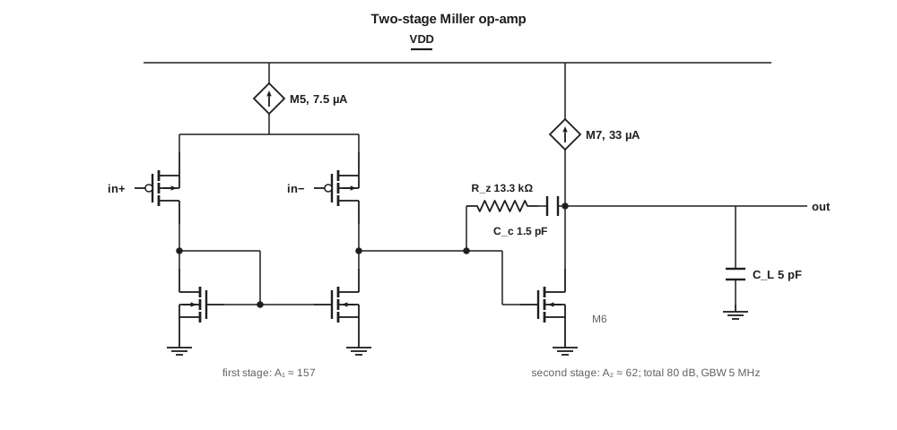
The first stage, the mirror-loaded pair of lesson 9, has gain A₁ = g_m1 R₁, where R₁ is the parallel output resistance of M2 and M4. The second stage, the common-source M6 with the current source M7 as its load, has gain A₂ = g_m6 R₂. Without compensation the two high-impedance nodes give two poles at similar, low frequencies, and the amplifier would be unstable in feedback. The Miller capacitor C_c across the second stage splits them. Its capacitance, multiplied by the second stage's gain, makes the first stage's output node very slow, which sets the dominant pole; and as frequency rises it shorts the second stage's gate to its drain, so M6 behaves like a diode and its output node becomes fast, pushing the second pole out to about g_m6/C_L.
The Miller capacitor also creates a zero. At high frequency the signal current fed forward through C_c from the first stage's output to the second stage's output opposes the current from M6, and at the frequency where they are equal the output vanishes. Because the feedforward current subtracts, the zero lies in the right half plane, where it adds phase lag like a pole while raising gain like a zero, the worst of both. In a MOS op-amp, whose g_m6 is modest, the zero sits uncomfortably close to the unity-gain frequency. The standard remedy is a nulling resistor R_z in series with C_c. With R_z = 1/g_m6 the zero moves to infinity; with a larger value it moves into the left half plane, and placing it on top of p₂ cancels the second pole entirely.
For a two-pole amplifier in unity feedback the phase margin is 90° minus the phase lag of the second pole at the unity-gain frequency, which is close to the GBW. A 60° margin needs p₂ at about 1.7 times the GBW, and the right-half-plane zero, if not removed, takes several degrees more.
A hand design procedure
Priya follows the procedure popularized by the textbook of Allen and Holberg and refined by many designers since, recast in gm/ID terms. Each step fixes one quantity from one requirement.
| Step | Requirement used | Quantity fixed |
|---|---|---|
| 1 | Phase margin and load | C_c ≥ about 0.22 C_L, so that p₂ can be placed beyond the GBW at reasonable g_m6 |
| 2 | Slew rate | Tail current I₅ = SR × C_c |
| 3 | Gain-bandwidth | g_m1 = 2π GBW C_c, hence g_m1/I_D for the input pair |
| 4 | Phase margin | g_m6 from p₂ = g_m6/C_L placed at the required multiple of GBW |
| 5 | Second-stage efficiency | I₆ from g_m6 and a chosen g_m6/I_D |
| 6 | Right-half-plane zero | R_z to cancel p₂ |
| 7 | DC gain and swing | Channel lengths of each device; check A₁A₂ and V_DSsat |
| 8 | Offset and noise | Input pair and load areas, from lesson 9 |
import math
# Two-stage Miller op-amp for the CX-1 reference buffer and preamp (illustrative process)
UT, n = 0.0259, 1.35
lam_per_um = 0.04
spec = {"GBW": 5e6, "CL": 5e-12, "SR": 5e6, "PM": 60}   # SR in V/s
# Step 1: Miller capacitor. Rule of thumb Cc >= 0.22 CL keeps p2 well beyond GBW
Cc = max(0.22 * spec["CL"], 1.0e-12)
Cc = math.ceil(Cc * 1e12 * 2) / 2 * 1e-12     # round up to 0.5 pF
# Step 2: tail current from slew rate
I5 = spec["SR"] * Cc
# Step 3: input gm from GBW
gm1 = 2 * math.pi * spec["GBW"] * Cc
g1 = gm1 / (I5 / 2)
# Step 4: second-stage gm from the phase margin. With p2 = gm6/CL and the zero cancelled,
# PM = 90 - atan(GBW/p2); 60 degrees needs p2 >= 1.73 GBW. Allow for the RHP zero with a nulling resistor.
p2_needed = math.tan(math.radians(90 - spec["PM"])) ** -1 * spec["GBW"]
gm6 = 2 * math.pi * p2_needed * spec["CL"] * 1.2          # 20 % margin for parasitics
# second stage at gm/ID = 10 /V
I6 = gm6 / 10
Rz = 1 / gm6 * (1 + spec["CL"] / Cc)   # moves the zero to cancel p2 (classic choice)
L1, L6 = 1.0, 0.5                      # first stage longer for gain; second stage short for speed
ro = lambda i, L: L / (lam_per_um * i)
A1 = gm1 * (ro(I5 / 2, L1) / 2)
A2 = gm6 * (ro(I6, L6) / 2)
A0 = A1 * A2
print(f"Cc = {Cc * 1e12:.1f} pF, I5 = {I5 * 1e6:.1f} uA, gm1 = {gm1 * 1e6:.0f} uS (gm/ID = {g1:.1f} /V)")
print(f"p2 needed >= {p2_needed / 1e6:.2f} MHz -> gm6 = {gm6 * 1e6:.0f} uS, I6 = {I6 * 1e6:.0f} uA")
print(f"nulling resistor Rz = {Rz / 1e3:.1f} kohm")
print(f"A1 = {A1:.0f}, A2 = {A2:.0f}, A0 = {A0:.0f} ({20 * math.log10(A0):.1f} dB)")
p1 = gm1 / (2 * math.pi * A0 * Cc)
print(f"dominant pole {p1:.0f} Hz; GBW check {A0 * p1 / 1e6:.2f} MHz")
# phase margin from the actual pole set with and without the nulling resistor
p2 = gm6 / (2 * math.pi * spec["CL"])
z_rhp = gm6 / (2 * math.pi * Cc)
f = spec["GBW"]
pm_plain = 90 - math.degrees(math.atan(f / p2)) - math.degrees(math.atan(f / z_rhp))
p_mirror = 60e6                        # mirror pole gm3/(2 pi 2Cgs3), estimated from sizing
c1 = 0.25e-12                          # parasitic capacitance at the first-stage output
p4 = 1 / (2 * math.pi * Rz * c1)       # pole created by Rz with that capacitance
pm_rz = 90 - math.degrees(math.atan(f / p_mirror)) - math.degrees(math.atan(f / p4))
print(f"p2 = {p2 / 1e6:.2f} MHz, RHP zero = {z_rhp / 1e6:.1f} MHz")
print(f"phase margin without Rz {pm_plain:.1f} deg")
print(f"with Rz: p2 cancelled; mirror pole {p_mirror / 1e6:.0f} MHz, Rz-C1 pole {p4 / 1e6:.1f} MHz -> PM {pm_rz:.1f} deg")
VDD = 1.8
print(f"supply current {(I5 + I6) * 1e6:.0f} uA, power {(I5 + I6) * VDD * 1e6:.0f} uW")Cc = 1.5 pF, I5 = 7.5 uA, gm1 = 47 uS (gm/ID = 12.6 /V) p2 needed >= 8.66 MHz -> gm6 = 326 uS, I6 = 33 uA nulling resistor Rz = 13.3 kohm A1 = 157, A2 = 62, A0 = 9817 (79.8 dB) dominant pole 509 Hz; GBW check 5.00 MHz p2 = 10.39 MHz, RHP zero = 34.6 MHz phase margin without Rz 56.1 deg with Rz: p2 cancelled; mirror pole 60 MHz, Rz-C1 pole 48.0 MHz -> PM 79.3 deg supply current 40 uA, power 72 uW
Working through the steps for the CX-1 specification: the Miller capacitor comes out at 1.5 pF after rounding up the 1.1 pF minimum. The slew rate then sets the tail current at 7.5 µA, and the GBW sets g_m1 at 47 µS, which with 3.75 µA per side is a g_m/I_D of 12.6 V⁻¹, in moderate inversion and a comfortable choice. For 60° of phase margin p₂ must be at least 8.7 MHz; allowing 20 % for parasitic capacitance at the output, g_m6 is 326 µS, which at g_m6/I_D = 10 V⁻¹ needs 33 µA in the second stage.
With the first stage at L = 1 µm and the second at 0.5 µm, the gains are 157 and 62, a total of about 9 800, or 80 dB, meeting the 75 dB requirement. The dominant pole falls at about 510 Hz, and the GBW checks at 5 MHz. Without a nulling resistor the right-half-plane zero sits at 35 MHz and the phase margin is 56°, short of the target. With R_z = 13.3 kΩ the zero cancels p₂, and the phase margin is then set by the next poles: the mirror pole of the first stage, about 60 MHz, and the new pole formed by R_z with the parasitic capacitance at the first stage's output, about 48 MHz. Together they leave a phase margin of about 79°. The op-amp draws 40 µA, 72 µW, which Priya reduces for the bandgap's internal amplifier, where 1 MHz is plenty, by scaling every current by five.
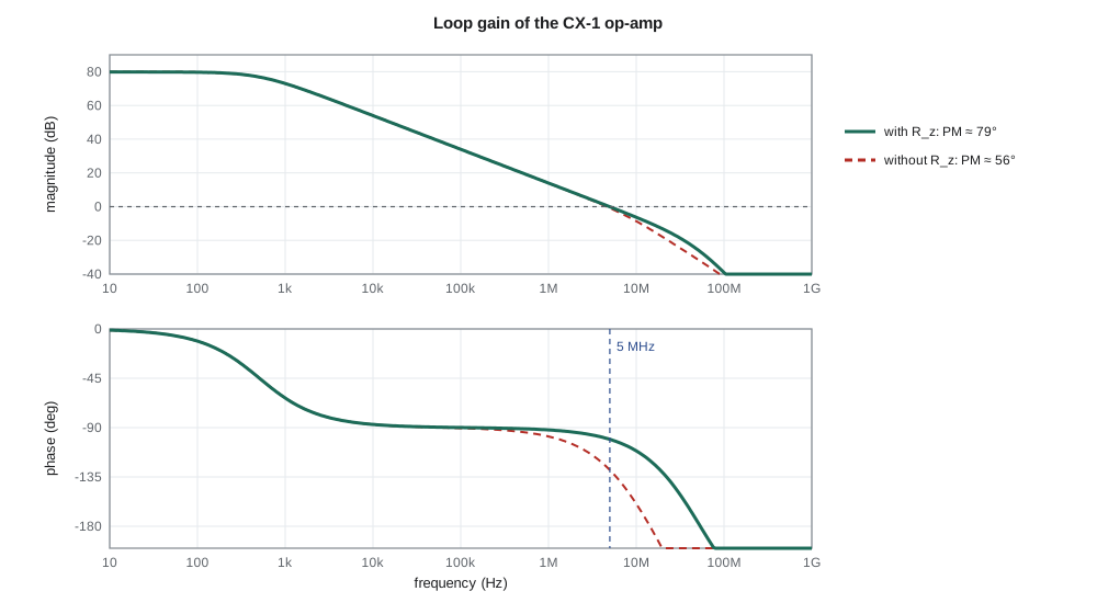
The resistor R_z is drawn in the same high-resistance poly as the bias generator's resistor, so that it tracks g_m6, which the constant-gm bias of lesson 8 makes proportional to 1/R. The cancellation therefore holds across process corners and temperature, which lesson 12's corner table confirms. A design in which R_z did not track g_m6 would see the zero drift away from p₂ at the corners, and its phase margin with it.
Worked problem
Slew rate and full-power bandwidth
The preamplifier must deliver a 1.2 V peak sine at up to 20 kHz. Is the 5 V/µs slew rate sufficient, and what is the largest frequency at which it could deliver that amplitude?
Show solution
- A sine of peak V_p at frequency f has a maximum slope 2πfV_p.
- \[2\pi \times 20\ \text{kHz} \times 1.2\ \text{V} = 0.15\ \text{V}/\mu\text{s} \ll 5\ \text{V}/\mu\text{s}\]
- \[f_{\max} = \frac{\text{SR}}{2\pi V_p} = \frac{5\times10^6}{2\pi \times 1.2} \approx 660\ \text{kHz}\]
Answer: The slew rate is more than thirty times what audio needs; it was set by the reference buffer, which must settle quickly after each data-converter conversion.
Output stage and swing
The second stage's output swings from V_DSsat of M6 above ground to V_DSsat of M7 below the supply, about 0.15 to 0.2 V from each rail at the chosen bias, which meets the 0.3 V specification. The input common-mode range of the PMOS pair runs from slightly below ground to about V_DD − |V_GS1| − V_DSsat5, roughly 1.0 V, which suits the microphone's ground-referred input but would not suit a follower with a rail-to-rail input. Rail-to-rail input op-amps place an NMOS pair in parallel with the PMOS pair and manage the transition between them, at the cost of an offset that changes with common-mode voltage.
The op-amp's output resistance is the parallel r_o of M6 and M7, about 190 kΩ, so it cannot drive a low-resistance load directly without losing gain. In CX-1 it sees only capacitive loads and feedback networks of several hundred kilohms, whose loading costs some of the 80 dB of open-loop gain but leaves plenty; the reference buffer's load is the capacitor array of the data converter.
The folded-cascode alternative
A folded-cascode op-amp is the main single-stage alternative. Its input pair's drain currents are folded into cascode devices of the opposite type and a cascoded mirror load, so the gain comes from one stage with very high output resistance, roughly (g_m r_o)², and the load capacitance itself compensates the amplifier: the only high-impedance node is the output, and the dominant pole is at the output. Higher load capacitance makes it more stable rather than less. Its non-dominant poles are at the low-impedance folding nodes, typically far above the GBW, so a folded cascode is faster for the same power when driving a capacitive load such as a switched-capacitor circuit, and it has no right-half-plane zero.
| Property | Two-stage Miller | Folded cascode |
|---|---|---|
| DC gain | High (A₁A₂), easily 75–85 dB | Moderate to high, 60–75 dB in one stage |
| Output swing | Within V_DSsat of each rail | Reduced by stacked cascodes, 2V_DSsat from each rail |
| Compensation | Miller C_c with nulling resistor | Load capacitance compensates |
| Effect of larger C_L | Lowers p₂ and phase margin | Lowers GBW but improves stability |
| Resistive loads | Possible with care | Poor without a buffer |
| Typical use | General purpose, buffers, audio | Switched-capacitor circuits, sample-and-holds |
For CX-1 the two-stage Miller op-amp wins: its output swing matters at 1.8 V, its gain is ample, and the uses, a preamplifier, a buffer and a bandgap loop, are general purpose. Had CX-1 included a switched-capacitor filter or a pipelined data converter, Priya would have designed a folded cascode for it as well.
Checks before layout
The hand design is a starting point. In simulation Priya checks the open-loop gain and phase across process corners and temperature, the closed-loop step response in unity gain with the full 5 pF load and with the actual feedback networks of each use, the slew rate in both directions, the power-supply rejection ratio, since supply noise from the digital half must not reach the output, and the offset in Monte Carlo with the Pelgrom statistics of lesson 7. She also runs a transient test of power-up, because a two-stage op-amp whose bias starts slowly can latch with its output at a rail when its feedback network is connected to a node that comes up first. Every one of those results goes into the design record for lesson 12's review.
Common mistakes
MistakeIgnoring the right-half-plane zero of the Miller op-amp.
InsteadIn MOS designs it sits close to the GBW and costs significant phase margin; use a nulling resistor.
MistakeMaking the nulling resistor from a different material from the bias resistor.
InsteadR_z must track 1/g_m6 across corners for the cancellation to hold.
MistakeRaising C_L on a two-stage op-amp without rechecking stability.
Insteadp₂ = g_m6/C_L falls with load capacitance, and the phase margin falls with it.
MistakeSetting the tail current from the GBW alone.
InsteadSlew rate, SR = I₅/C_c, often sets the tail current instead.
Summary and key terms
- The Miller capacitor splits the two-stage op-amp's poles: p₁ ≈ 1/(A₂R₁C_c), GBW = g_m1/C_c, p₂ ≈ g_m6/C_L.
- The feedforward path through C_c creates a right-half-plane zero at g_m6/C_c; a nulling resistor moves or cancels it.
- A hand procedure fixes C_c, I₅, g_m1, g_m6, I₆, R_z and channel lengths from the specification one step at a time.
- The CX-1 design gives 80 dB, 5 MHz, 5 V/µs and about 79° phase margin at 40 µA.
- A constant-gm bias with a matched R_z keeps the cancellation and the GBW stable across corners.
- The folded cascode is compensated by its load and suits switched-capacitor circuits; the two-stage design gives more swing and gain.
- Miller compensation
- Placing a capacitor across an inverting gain stage to split the amplifier's poles.
- Gain-bandwidth product
- The product of DC gain and dominant pole frequency, g_m1/C_c for a Miller op-amp.
- Right-half-plane zero
- A zero with positive real part, which adds phase lag while raising gain.
- Nulling resistor
- A resistor in series with the Miller capacitor that moves or cancels the zero.
- Slew rate
- The maximum rate of change of an amplifier's output, I₅/C_c for a Miller op-amp.
- Phase margin
- 180° plus the loop-gain phase at the unity-gain frequency.
- Folded cascode
- A single-stage op-amp whose input currents are folded into cascode devices of the opposite type.
- Power-supply rejection
- The ratio of the gain from input to output to the gain from supply to output.
Practice problems
Work each problem on paper first, then reveal the answer to check.
A Miller op-amp has g_m1 = 60 µS and C_c = 2 pF. Find its GBW.
Show answer
60 µS/(2π × 2 pF) ≈ 4.8 MHz.
Find the slew rate for I₅ = 10 µA and C_c = 2 pF.
Show answer
5 V/µs.
With g_m6 = 400 µS, C_L = 4 pF and C_c = 1 pF, find p₂ and the RHP zero frequency.
Show answer
p₂ ≈ 15.9 MHz; z ≈ 63.7 MHz.
What R_z cancels p₂ in the previous problem?
Show answer
(1/400 µS)(1 + 4) = 12.5 kΩ.
A two-pole loop has its second pole at twice the unity-gain frequency. Estimate its phase margin.
Show answer
90° − atan(0.5) ≈ 63°.
Why does a larger load capacitance help the stability of a folded cascode?
Show answer
The output is its dominant pole, so more C_L lowers the unity-gain frequency relative to the non-dominant poles.
Lesson quiz · 5 questions
Score 60% or more to complete this lesson.
Create a free account to save your progress, take quizzes and earn a certificate.