
ELE-445 · Lesson 8 of 12 · 22 min
Current mirrors and voltage references
Every analog block on CX-1 starts from two things that the rest of the chip takes for granted: a reference current to bias its transistors and a reference voltage against which signals are measured. The data converter's accuracy can be no better than its reference; the op-amp's bandwidth and power follow its bias current. This lesson designs both at the transistor level. ELE-340 studied current mirrors built from discrete or integrated bipolar devices and introduced the bandgap idea; here the mirrors are MOS devices sized with the gm/ID method, the bias generator must hold the analog blocks' transconductances constant across process and temperature, and the bandgap reference is designed for the CX-1 converter.
The MOS current mirror on a chip
A simple NMOS mirror connects a diode-connected reference transistor M1, with gate tied to drain, to the gate of an output transistor M2. If both are in saturation, have the same V_GS and the same size, they carry the same current; scaling M2's width by k scales the output by k. The copy is imperfect for three reasons, and each has an IC-design remedy.
The first is channel-length modulation. M1's drain sits at V_GS while M2's sits wherever the load puts it, and the difference in V_DS changes the current by λ times that difference. The output resistance is r_o of M2, which lesson 3 showed grows with channel length; mirror devices on CX-1 are drawn at 1 to 2 µm. The second is threshold mismatch, which causes a current error of (g_m/I_D)ΔV_T; mirrors are therefore biased at low g_m/I_D, about 8 to 10 V⁻¹, and drawn with enough area for their accuracy. The third is systematic layout error: a mirror ratio of four is drawn as one unit and four units, all identical, in a common-centroid array, never as one transistor four times as wide, so that edge effects scale exactly.
Cascode mirrors
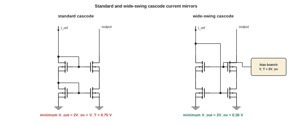
Where a single transistor's output resistance is not enough, a cascode stacks a second transistor M4 above the output device. M4's gate is held at a fixed voltage, so it holds M2's drain nearly constant whatever happens above it, and the output resistance rises by roughly the cascode device's intrinsic gain.
import math
# 1. Output resistance of simple and cascode NMOS mirrors at 10 uA
I = 10e-6
lam_per_um = 0.04          # lambda * L in um/V for the illustrative process
gm = 150e-6                # from the gm/ID sizing of lesson 3
for L in (0.5, 1.0, 2.0):
    ro = L / (lam_per_um * I)
    rc = gm * ro * ro      # cascode: about gm ro^2
    print(f"L = {L} um: simple ro = {ro / 1e6:.2f} Mohm, cascode ~ {rc / 1e9:.2f} Gohm")

# 2. Headroom: simple cascode versus wide-swing cascode (Vov = 0.15 V, VT = 0.45 V)
vov, vt = 0.15, 0.45
print(f"minimum output voltage: standard cascode {2 * vov + vt:.2f} V, wide-swing {2 * vov:.2f} V")

# 3. Bandgap reference: VBE of a substrate PNP plus a scaled PTAT voltage
k_q = 8.617e-5             # Boltzmann constant over charge, V/K
vg0, eta = 1.205, 3.5       # extrapolated bandgap, temperature exponent of saturation current
def vbe(T, ic=2e-6, T0=300.0, vbe0=0.680):
    # VBE(T) = VG0 - (VG0 - VBE0) T/T0 - eta (kT/q) ln(T/T0)   (constant collector current)
    return vg0 - (vg0 - vbe0) * T / T0 - eta * k_q * T * math.log(T / T0)
N = 8                      # emitter area ratio of the PTAT pair
dvbe_coeff = k_q * math.log(N)       # V per kelvin
dvbe_dT = (vbe(301) - vbe(299)) / 2
gain = -dvbe_dT / dvbe_coeff         # resistor ratio that cancels the slope at 300 K
print(f"dVBE/dT at 300 K = {dvbe_dT * 1e3:.2f} mV/K; PTAT slope (k/q) ln {N} = {dvbe_coeff * 1e6:.1f} uV/K")
print(f"required PTAT gain = {gain:.2f}")
temps = list(range(-40, 126, 5))
vref = [vbe(t + 273.15) + gain * dvbe_coeff * (t + 273.15) for t in temps]
print(f"Vref at -40/25/125 C: {vref[0]:.4f} / {vref[temps.index(25)]:.4f} / {vref[-1]:.4f} V")
spread = max(vref) - min(vref)
tc = spread / (sum(vref) / len(vref)) / (temps[-1] - temps[0]) * 1e6
print(f"spread {spread * 1e3:.2f} mV over -40..125 C -> box-method TC {tc:.1f} ppm/C")
tpk = temps[vref.index(max(vref))]
print(f"peak at {tpk} C (curvature from the T ln T term)")L = 0.5 um: simple ro = 1.25 Mohm, cascode ~ 0.23 Gohm L = 1.0 um: simple ro = 2.50 Mohm, cascode ~ 0.94 Gohm L = 2.0 um: simple ro = 5.00 Mohm, cascode ~ 3.75 Gohm minimum output voltage: standard cascode 0.75 V, wide-swing 0.30 V dVBE/dT at 300 K = -2.05 mV/K; PTAT slope (k/q) ln 8 = 179.2 uV/K required PTAT gain = 11.45 Vref at -40/25/125 C: 1.2930 / 1.2955 / 1.2911 V spread 4.39 mV over -40..125 C -> box-method TC 20.5 ppm/C peak at 25 C (curvature from the T ln T term)
At 10 µA a simple mirror device at L = 1 µm has an output resistance of 2.5 MΩ; with a cascode the output resistance is about 0.9 GΩ. The price is headroom. A standard cascode, in which the cascode gate is biased by another diode-connected stack, needs the output to sit at least 2V_ov + V_T above ground, about 0.75 V in the script's example. On a 1.8 V supply that is almost half the swing gone. The wide-swing cascode biases the cascode gate at only V_T + 2V_ov, from a separate small branch, so that M2 sits just at the edge of saturation and the output can swing to within 2V_ov of the rail, about 0.3 V.
Generating the reference current
Mirrors copy a current; something must create it. A resistor from the supply to a diode-connected transistor gives a current that varies with the supply, the threshold and the resistor, and is good enough only for non-critical uses. A self-biased circuit removes the supply dependence by making the current define itself. The most widely used in CMOS is the constant-gm, or beta-multiplier, reference: two NMOS devices with a width ratio K, one with a source resistor R, are forced to carry equal currents by a PMOS mirror above them. The only consistent current is the one that makes the extra V_GS of the smaller device equal to the drop across R, which gives a closed-form result in strong inversion.
The striking result is the second equation: the transconductance of the reference device depends only on R and K, not on mobility, threshold or supply. Any transistor biased from this reference with the same inversion level and a scaled size has a transconductance that tracks 1/R. That is exactly what an op-amp's bandwidth needs, because the gain-bandwidth product is g_m/C_c: with a constant-gm bias it becomes proportional to 1/(RC), and its spread is set by the resistor and capacitor alone, about ±20 % and ±10 %, rather than by the much larger spread of the transistors. Lesson 12 shows the effect in the corner simulations of the CX-1 op-amp. Self-biased references have a second, degenerate operating point at zero current, so every one needs a start-up circuit that injects a little current at power-up and then switches itself off; forgetting it is a classic first-silicon failure.
The bandgap reference
The CX-1 data converter needs a voltage reference stable to a few millivolts from −40 °C to 125 °C. Every practical on-chip reference of this kind is a bandgap: it adds a voltage that falls with temperature to one that rises with temperature, in proportions that cancel. The falling voltage is the base-emitter voltage of a bipolar transistor, which decreases by about 2 mV/K. The rising voltage is the difference between the V_BE values of two bipolar transistors run at different current densities, which is proportional to absolute temperature (PTAT).
A CMOS process has no designed bipolar transistors, but it has a parasitic one that works well for references: the vertical PNP formed by a p+ diffusion in an n-well, which acts as the emitter, the n-well as the base and the substrate as the collector. Its collector is permanently tied to the substrate, which suits a diode-connected use. A typical CMOS bandgap uses one unit PNP and a group of N identical units in parallel, eight in the common arrangement of one centre unit surrounded by eight in a three-by-three array, so that the units are common-centroid. An op-amp forces the two branches to the same voltage, and the ΔV_BE appears across a resistor; mirroring that PTAT current through a larger resistor and adding V_BE gives the reference.
The code models V_BE with the standard expression for a junction at constant current, including the curvature term that comes from the temperature dependence of the saturation current. At 300 K it gives dV_BE/dT ≈ −2.05 mV/K. The PTAT term with N = 8 has a slope of k/q × ln 8 ≈ 179 µV/K, so a gain of about 11.4 cancels the slope at room temperature.
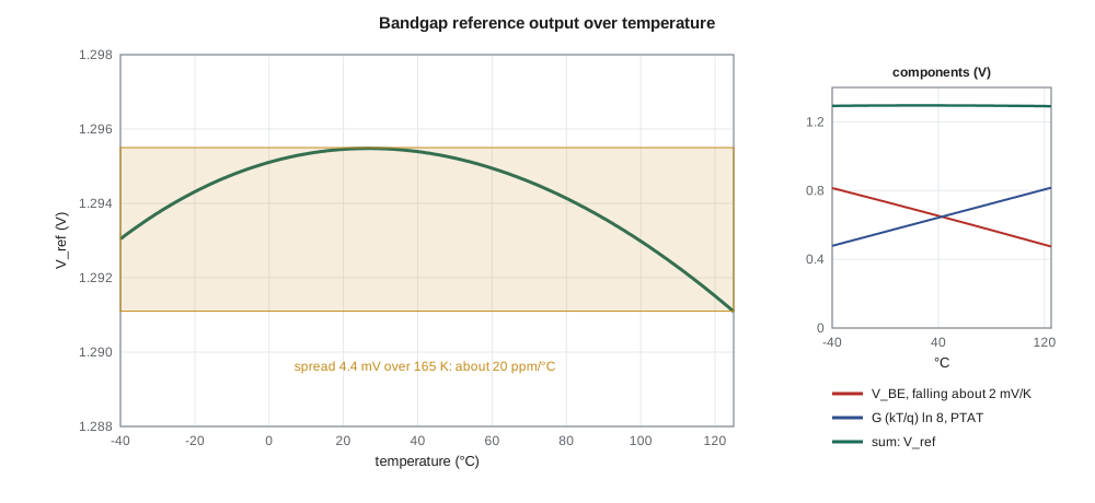
The result is a reference of about 1.295 V that varies by 4.4 mV across the full 165 K range, a box-method temperature coefficient of about 20 ppm/°C, inside the CX-1 specification of 30 ppm/°C. The remaining variation is a downward-opening parabola with its peak near the temperature where the slopes were cancelled. Curvature-correction schemes, which add a small term proportional to T ln T or use a second, nonlinear current, can reduce it several-fold where a converter needs it, at the cost of complexity that CX-1's 10 bits do not justify.
The output voltage is close to the silicon bandgap voltage extrapolated to absolute zero, about 1.2 V, plus a term from the curvature, which is how the circuit got its name. A useful check on any bandgap design is that the optimized output lands in the range 1.2 to 1.3 V. A design that cancels the slope at 1.4 V has a modelling error somewhere.
What limits a bandgap's accuracy
The temperature coefficient is the easy part. The absolute value of a bandgap varies from chip to chip, mainly because of the op-amp's offset and the mismatch of the PNP devices and resistors. The op-amp's offset appears at the output multiplied by roughly the PTAT gain G, about eleven here, so an op-amp offset of 2 mV moves the output by 22 mV, nearly 2 %. Three remedies are used together. The op-amp's input pair is drawn large and in common centroid, to reduce its offset. The circuit is made chopper-stabilized or uses a larger ΔV_BE, so the gain is smaller. And the output is trimmed after manufacture: a few bits of programmable resistor ratio, set at production test by blowing fuses or writing a one-time-programmable memory, adjust each chip to its target. Lesson 12's Monte Carlo analysis shows that untrimmed, only about 60 % of CX-1 parts would be within 10 mV of nominal, while a 4-bit trim brings more than 99 % within 3 mV.
Worked problem
PTAT gain and op-amp offset
A bandgap uses N = 8 and has V_BE = 0.68 V at 27 °C with a slope of −2.0 mV/K. Find the PTAT gain that cancels the slope, the output voltage, and the output shift caused by a 1.5 mV op-amp offset.
Show solution
- \[G\,\frac{k}{q}\ln 8 = 2.0\ \text{mV/K} \;\Rightarrow\; G = \frac{2.0\times10^{-3}}{8.617\times10^{-5}\times2.079} = 11.2\]
- \[V_{\text{ref}} = 0.68 + 11.2 \times 0.0259 \times 2.079 = 0.68 + 0.603 = 1.283\ \text{V}\]
- An offset in the loop that defines ΔV_BE is amplified by about G: 11.2 × 1.5 mV ≈ 17 mV.
Answer: G ≈ 11.2, V_ref ≈ 1.28 V, and a 1.5 mV offset shifts the output by about 17 mV, which is why bandgaps are trimmed.
The CX-1 bias and reference block
Priya's final block diagram combines the pieces. A beta-multiplier generates a master current with a constant-gm characteristic and a start-up circuit; wide-swing cascode mirrors distribute scaled copies to every analog block, each copy drawn from units in a common-centroid array and switched off when its block is powered down. A separate PTAT current from the bandgap core feeds the blocks, such as the comparator, whose behaviour should track temperature in a particular way. The bandgap output, about 1.295 V and trimmable in 4 mV steps, is buffered by a small op-amp to drive the data converter's reference input, whose capacitor array draws charge in pulses that the bandgap core itself could not supply. The whole block draws about 14 µA from the 1.8 V supply, 25 µW, the number used in lesson 6's budget.
Common mistakes
MistakeDrawing a ratioed mirror as one wide output transistor.
InsteadUse identical units so that edge effects and layout errors scale exactly with the ratio.
MistakeUsing a standard cascode on a low supply without checking headroom.
InsteadIt needs 2V_ov + V_T at the output; a wide-swing cascode needs only about 2V_ov.
MistakeOmitting the start-up circuit in a self-biased reference.
InsteadThe circuit can rest at zero current; a start-up circuit forces it to the correct operating point.
MistakeExpecting a bandgap's absolute value to be accurate without trim.
InsteadOp-amp offset multiplied by the PTAT gain sets the spread; trim each part.
Summary and key terms
- MOS mirrors copy currents with errors from channel-length modulation, threshold mismatch and layout; long devices at low g_m/I_D in common-centroid arrays reduce them.
- Cascodes raise output resistance to about g_m r_o²; wide-swing cascodes save one threshold of headroom.
- A constant-gm reference makes transconductance depend on a resistor, so amplifier bandwidth depends on R and C rather than on transistor parameters.
- Self-biased references need start-up circuits.
- A bandgap adds a falling V_BE to a rising, scaled ΔV_BE = (kT/q)ln N to give about 1.2–1.3 V with low temperature drift.
- Curvature leaves a parabolic residue; offset amplified by the PTAT gain sets the absolute spread, which trimming removes.
- Cascode
- A transistor stacked above another to hold its drain voltage constant and raise output resistance.
- Wide-swing cascode
- A cascode biased so that the lower device sits at the edge of saturation, maximizing output swing.
- Constant-gm reference
- A self-biased current reference that makes device transconductance proportional to 1/R.
- Start-up circuit
- A circuit that moves a self-biased reference away from its zero-current state at power-up.
- PTAT
- Proportional to absolute temperature.
- Bandgap reference
- A voltage reference that cancels the temperature coefficients of V_BE and a PTAT voltage.
- Vertical PNP
- A parasitic bipolar transistor formed by p+ diffusion, n-well and substrate in CMOS.
- Trim
- Adjustment of each part after manufacture to correct its absolute value.
Practice problems
Work each problem on paper first, then reveal the answer to check.
A mirror device at L = 2 µm carries 5 µA with λL = 0.04 µm/V. Find r_o.
Show answer
λ = 0.02 V⁻¹; r_o = 1/(0.02 × 5 µA) = 10 MΩ.
With g_m = 100 µS and r_o = 5 MΩ for both devices, estimate a cascode's output resistance.
Show answer
100 µS × 5 MΩ × 5 MΩ = 2.5 GΩ.
Find kT/q × ln N at 300 K for N = 24.
Show answer
0.02585 × 3.18 ≈ 82 mV.
A beta-multiplier has K = 4 and R = 20 kΩ. Find g_m1.
Show answer
(2/20 kΩ)(1 − 1/2) = 50 µS.
Why does a constant-gm bias make an op-amp's GBW depend on R and C only?
Show answer
GBW = g_m/(2πC_c) and g_m ∝ 1/R.
A bandgap has PTAT gain 10. What output shift does a 3 mV op-amp offset cause?
Show answer
About 30 mV.
Lesson quiz · 5 questions
Score 60% or more to complete this lesson.
Create a free account to save your progress, take quizzes and earn a certificate.