
ELE-445 · Lesson 5 of 12 · 21 min
Static CMOS logic and logical effort
The inverter generalizes directly to every other static CMOS gate. Each gate has a pull-down network of NMOS transistors between its output and ground and a pull-up network of PMOS transistors between its output and the supply, arranged so that for every input combination exactly one network conducts. This lesson builds NAND, NOR and compound gates, sizes them so that they drive as well as an inverter, and introduces logical effort, a method for estimating and minimizing the delay of a path of gates with nothing more than arithmetic. Amara uses it to check the one awkward net in the CX-1 counters, a clock-enable signal that must reach 64 flip-flops in time.
Complementary networks
In a NAND gate the pull-down network is two NMOS transistors in series, so the output is pulled low only when both inputs are high; the pull-up network is two PMOS transistors in parallel, so the output is pulled high if either input is low. A NOR gate is the dual: parallel NMOS and series PMOS. The rule for any static CMOS gate is that the pull-up network is the series-parallel dual of the pull-down network: series connections in one become parallel connections in the other. A compound gate such as an AND-OR-INVERT, which computes the complement of AB + C, is built the same way: in the pull-down network, A and B in series, in parallel with C; in the pull-up network, A and B in parallel, in series with C.
Static CMOS gates are naturally inverting. A single stage of CMOS can only compute functions that pull the output low when inputs go high, so a non-inverting AND is built as a NAND followed by an inverter. Synthesis tools know this and prefer inverting gates; a designer reading a netlist sees mostly NANDs, NORs and AOIs.
Sizing for equal drive
A gate should drive its output as strongly as a reference inverter, in the worst case. The reference inverter in this lesson has an NMOS of unit width and a PMOS of width 2, a compromise between equal rise and fall delays, which would need a ratio near four in this process, and smaller area. Transistors in series add resistance, so each must be wider in proportion. In a two-input NAND the two series NMOS devices are each made width 2, so that their series resistance equals the unit NMOS; the parallel PMOS devices stay at width 2, because in the worst case only one of them is on. In a two-input NOR the series PMOS devices become width 4 and the parallel NMOS stay at 1.
| Gate | NMOS widths | PMOS widths | Input capacitance (units) | Logical effort g | Parasitic delay p |
|---|---|---|---|---|---|
| Inverter | 1 | 2 | 3 | 1 | 1 |
| NAND2 | 2, 2 (series) | 2, 2 (parallel) | 4 | 4/3 | 2 |
| NAND3 | 3, 3, 3 | 2, 2, 2 | 5 | 5/3 | 3 |
| NOR2 | 1, 1 (parallel) | 4, 4 (series) | 5 | 5/3 | 2 |
| NOR3 | 1, 1, 1 | 6, 6, 6 | 7 | 7/3 | 3 |
| AOI21 | 2, 2 (series) and 1 | 4, 4 (parallel) and 4 | 6 (A, B); 5 (C) | 2 (A, B); 5/3 (C) | 7/3 |
The table shows why NAND gates are preferred to NOR gates in CMOS. With slower PMOS devices, putting them in series costs much more width than putting NMOS devices in series. A NOR2 presents 5 units of input capacitance for the drive of an inverter that presents 3; a NAND2 presents only 4. NOR gates with more than three or four inputs are rarely used, and wide functions are built from trees of smaller gates.
Logical effort
Logical effort, developed by Ivan Sutherland and Robert Sproull and published as a book with David Harris in 1999, turns the RC delay model of lesson 4 into a simple algebra of gate delays. The delay of a gate, measured in units of τ, the delay of an ideal inverter driving an identical inverter with no parasitics, is the sum of two parts: an effort delay that depends on the load, and a parasitic delay that depends on the gate itself.
The electrical effort h is the ratio of the gate's load capacitance to its own input capacitance, its fan-out in capacitance terms. The logical effort g says how much worse the gate is than an inverter at producing output current for a given input capacitance; it is the gate's input capacitance divided by the inverter's, for equal drive. From the table, a NAND2 has g = 4/3 and a NOR2 g = 5/3. The parasitic delay p comes from the gate's own drain capacitance, roughly proportional to the number of transistors connected to its output. For the illustrative CX-1 process τ is about 15 ps, so an inverter driving four copies of itself has a delay of (1 × 4 + 1)τ = 5τ, about 75 ps: the FO4 delay of lesson 4.
For a path of N gates the method extends neatly. The path logical effort G is the product of the gates' logical efforts. The path electrical effort H is the ratio of the final load to the path's input capacitance. A branching effort B accounts for any gate whose output also drives loads off the path. The product F = GBH is the path effort, and it is fixed by the logic and the loads, independent of how the gates in between are sized. The path delay is minimized when every stage bears the same effort, F^{1/N}, and the minimum delay follows directly.
Sizing then proceeds backwards from the load: each gate's input capacitance is its logical effort times its output load divided by the stage effort. The method's beauty is that a designer can size a path on a sheet of paper and know the answer is within a few percent of the optimum that a simulator would find.
The CX-1 enable path
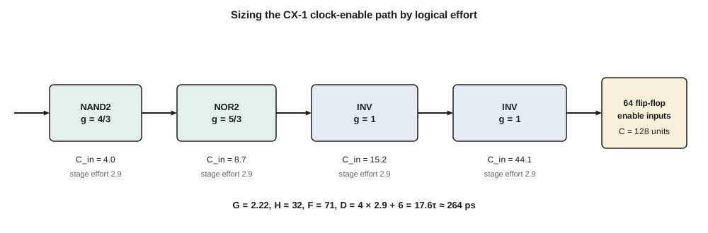
The counter block has one net that the synthesis tool flags as slow. A register bit, decoded with a NAND2 and a NOR2 from other control signals, must drive the clock-enable input of all 64 flip-flops in the period counters, and each enable input presents about two units of capacitance. The register output can drive a gate of 4 units. The path is NAND2, NOR2, then two inverters to restore the polarity and drive the load.
import math
# Logical effort: size the path from a register output to the 64 loads of a clock-enable net
tau = 15e-12          # process time unit for the illustrative 180 nm process, s
p_inv = 1.0           # parasitic delay of an inverter, in units of tau

# Path: NAND2 -> NOR2 -> inverter -> inverter, driving 64 flip-flop enable inputs
stages = [("NAND2", 4 / 3, 2.0), ("NOR2", 5 / 3, 2.0), ("INV", 1.0, 1.0), ("INV", 1.0, 1.0)]
c_in = 4.0            # input capacitance of the first gate, in unit-inverter inputs
c_out = 64 * 2.0      # each enable input looks like two unit inverters
G = math.prod(g for _, g, _ in stages)
H = c_out / c_in
B = 1.0               # no branching inside the path
F = G * B * H
N = len(stages)
f_hat = F ** (1 / N)
P = sum(p for _, _, p in stages)
D = N * f_hat + P
print(f"G = {G:.3f}, H = {H:.1f}, path effort F = {F:.1f}")
print(f"best stage effort f = {f_hat:.2f}; delay D = {D:.1f} tau = {D * tau * 1e12:.0f} ps")
# input capacitance of each stage, working back from the load
c = c_out
sizes = []
for name, g, p in reversed(stages):
    c = c * g / f_hat
    sizes.append((name, c))
for name, cin in reversed(sizes):
    print(f"  {name:<5} input capacitance {cin:6.1f} units")
# How many stages would be best?  Compare N = 2..7 with extra inverters (keeping the logic)
print("stages  delay (tau)")
for n_tot in range(3, 8):
    f = F ** (1 / n_tot)
    d = n_tot * f + P + (n_tot - N) * p_inv
    print(f"  {n_tot}     {d:5.1f}")
best = math.log(F) / math.log(3.59)
print(f"best stage count from ln F / ln 3.59: {best:.1f}")G = 2.222, H = 32.0, path effort F = 71.1 best stage effort f = 2.90; delay D = 17.6 tau = 264 ps NAND2 input capacitance 4.0 units NOR2 input capacitance 8.7 units INV input capacitance 15.2 units INV input capacitance 44.1 units stages delay (tau) 3 17.4 4 17.6 5 18.7 6 20.2 7 21.9 best stage count from ln F / ln 3.59: 3.3
The path logical effort is 4/3 × 5/3 × 1 × 1 = 2.22 and the electrical effort is 128/4 = 32, so the path effort is about 71. With four stages, each stage should bear an effort of 71^{1/4} ≈ 2.9, and the path delay is 4 × 2.9 + 6 = 17.6τ, about 264 ps. Working back from the load, the final inverter needs an input capacitance of 44 units, the one before it 15, and the NOR2 about 9. The comparison of stage counts shows that three stages would be very slightly faster, but removing an inverter would invert the signal, so four is the right choice.
A well-known result of the method is that the best stage effort is about 4 when parasitic delays are included, which is why chains of buffers driving large loads taper by a factor of about four per stage. The best number of stages is roughly the logarithm of the path effort to base 4, or slightly less. A path effort of 71 gives about three stages. The fan-out-of-four convention for the FO4 delay comes from the same result.
Amara's conclusion is reassuring and typical. The 264 ps path delay is a tiny fraction of CX-1's 50 ns clock period, so the path was never at risk; the synthesis tool flagged it because its default buffer choice was a single ×1 inverter driving all 64 loads, with an electrical effort of 43 in one stage and a delay of about 44τ, roughly 0.66 ns, plus a slow edge that would have increased short-circuit power in all 64 flip-flops. She lets the tool rebuild the net as a small buffer tree, which is what its optimization step does once the constraint is set.
Worked problem
Choosing between NAND and NOR implementations
A signal must be the AND of four inputs and drive a load of 60 units from an input capacitance of 5 units. Compare a NAND4 followed by an inverter with two NAND2 gates feeding a NOR2. Take g = 2 and p = 4 for the NAND4.
Show solution
- NAND4 + INV: G = 2 × 1 = 2, H = 12, F = 24, N = 2, P = 4 + 1 = 5.
- \[D = 2\sqrt{24} + 5 = 9.8 + 5 = 14.8\ \tau\]
- NAND2 + NOR2: G = 4/3 × 5/3 = 2.22, H = 12, F = 26.7, N = 2, P = 2 + 2 = 4.
- \[D = 2\sqrt{26.7} + 4 = 10.3 + 4 = 14.3\ \tau\]
Answer: The two-level version is slightly faster because its parasitic delay is smaller, even though its logical effort is higher. With a larger load the NAND4 version would win, because effort delay would dominate.
Beyond static CMOS
Static CMOS is not the only way to build logic, though it is the default. Pass-transistor logic uses transistors as switches to steer signals, saving devices for functions such as multiplexers and XOR gates, but it degrades logic levels: an NMOS switch can pass a low cleanly but passes a high only to V_DD − V_T. Transmission gates, an NMOS and PMOS in parallel driven by complementary signals, pass both levels fully and are the basis of most flip-flops and multiplexers in standard cell libraries. Dynamic logic precharges a node and conditionally discharges it, giving fast, compact gates, but it needs a clock, is sensitive to noise and charge sharing, and draws power every cycle; it is found in high-performance processor datapaths rather than in chips like CX-1. For CX-1 every gate is static CMOS from the library.
Logic synthesis and what it does with gates
When Amara synthesizes the counter block, the synthesis tool performs at scale what this lesson did by hand. It translates the hardware description into a network of generic logic, optimizes the Boolean expressions, maps them onto library cells and chooses each cell's drive strength to meet the timing constraints at minimum area or power. Its choices are driven by the same quantities as logical effort: input capacitance, drive and parasitic delay, all read from the library's characterization tables rather than from simple ratios. A designer who understands logical effort can read the tool's choices critically. When a timing report shows a 0.7 ns delay through one inverter, the cause is obvious: too much load on too small a gate.
Common mistakes
MistakeMaking every transistor in a NOR gate the same width as in the inverter.
InsteadSeries devices need proportionally more width, or the gate will be slower than the reference.
MistakeDriving a large load with a single minimum inverter.
InsteadAn electrical effort of tens gives a slow delay and slow edges; taper with a buffer chain.
MistakeUsing a long NOR chain in CMOS.
InsteadSeries PMOS devices make NOR gates expensive; prefer NAND-based logic.
MistakeAdding buffer stages without limit.
InsteadEach stage adds parasitic delay; the best stage effort is about 4.
Summary and key terms
- Static CMOS gates have complementary pull-up and pull-down networks; series in one is parallel in the other.
- Series transistors are widened to keep a gate's worst-case drive equal to the reference inverter's.
- NAND gates have lower logical effort than NOR gates in CMOS because PMOS devices are slower.
- Gate delay is d = gh + p in units of τ; the path effort F = GBH is fixed by the logic and the loads.
- Path delay is minimized with equal stage effort F^{1/N}, and the best stage effort is about 4.
- Synthesis tools apply the same principles using characterized library tables.
- Pull-down network
- The NMOS transistors that connect a gate's output to ground.
- Pull-up network
- The PMOS transistors that connect a gate's output to the supply.
- Logical effort
- The ratio of a gate's input capacitance to an inverter's for the same output drive.
- Electrical effort
- The ratio of a gate's load capacitance to its input capacitance.
- Parasitic delay
- The part of a gate's delay caused by its own output capacitance.
- Path effort
- F = GBH, the product of the path's logical, branching and electrical efforts.
- Transmission gate
- Parallel NMOS and PMOS switches that pass both logic levels fully.
- Compound gate
- A single static CMOS gate implementing an AND-OR or OR-AND function with inversion.
Practice problems
Work each problem on paper first, then reveal the answer to check.
An inverter drives a load of 24 units from an input capacitance of 3 units. Find its delay in τ.
Show answer
h = 8, so d = 8 + 1 = 9τ.
Find the logical effort of a three-input NOR sized with a PMOS/NMOS ratio of 2.
Show answer
Input capacitance 6 + 1 = 7 versus 3, so g = 7/3.
A path has F = 256. How many stages minimize its delay, and what is the stage effort?
Show answer
About 4 stages, each with effort 4.
Size the input capacitance of an inverter that drives 60 units with stage effort 4.
Show answer
60/4 = 15 units.
Why is a NAND2 preferred to a NOR2 in CMOS?
Show answer
Its logical effort is 4/3 rather than 5/3, because series NMOS devices cost less width than series PMOS.
What is the FO4 delay in τ for an inverter with p = 1?
Show answer
5τ.
Lesson quiz · 5 questions
Score 60% or more to complete this lesson.
Create a free account to save your progress, take quizzes and earn a certificate.