
ELE-340 · Lesson 4 of 12 · 25 min
Operational amplifier internal design
Circuit analysis courses treat the op amp as an ideal block with infinite gain, infinite input resistance and zero output resistance. Real op amps come close because of how they are built inside, from the pieces of the last three lessons: a differential pair with a current-mirror load at the input, a high-gain voltage amplifier stage in the middle, a low-output-resistance buffer at the end, and a network of mirrors that biases everything. Knowing that structure explains the datasheet: why the open-loop gain is about a hundred thousand or more, why it falls with frequency from a few hertz upward, why the output cannot change faster than a certain number of volts per microsecond, and why the inputs draw a little current and have a little offset. This lesson builds a two-stage op amp, calculates its gain, bandwidth and slew rate, and reads those results back into datasheet terms.
Amara has a practical reason to care. The APS-2 needs three op amps: the hum-rejecting receiver, the preamplifier and the driver at the front of the power amplifier. The last one must swing 8 V peak into the power stage at voice frequencies, and an op amp chosen for its low cost and low supply current may not be able to change its output quickly enough. Before choosing a part, she works out what limits an op amp's speed.
The architecture of an op amp
Most op amps follow one of two plans. The classic bipolar design introduced in the late 1960s has three stages: a differential input stage with an active load, a high-gain intermediate stage with a compensation capacitor, and a class-AB emitter-follower output stage. Most CMOS op amps use two stages: a differential pair with a mirror load, and a common-source gain stage with a compensation capacitor that doubles as the output stage, sometimes followed by a buffer. In both, almost all the voltage gain comes from two high-impedance nodes, one at the output of each gain stage.
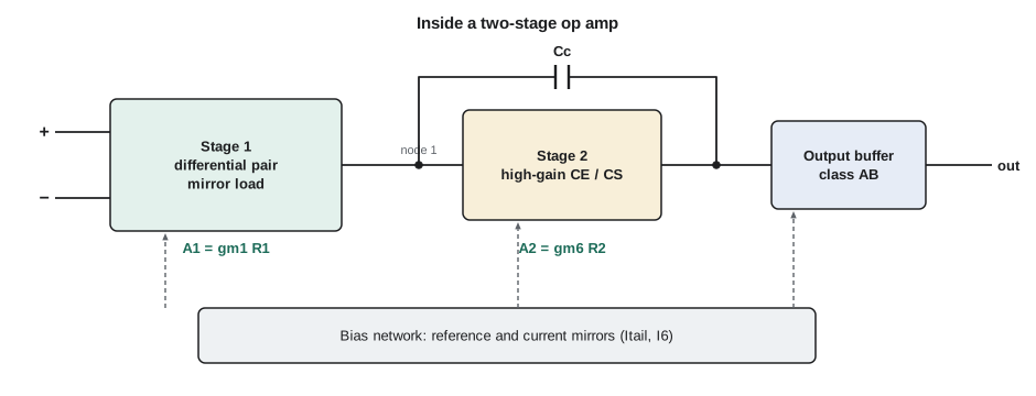
DC gain of a two-stage op amp
Stage 1 is the actively loaded pair of lesson 3. Its gain is g_m1 times the total resistance at node 1: the output resistances of the pair transistor and the mirror in parallel with the input resistance of stage 2. Stage 2 is an actively loaded common-emitter or common-source stage, whose gain is g_m6 times the resistance at the output node. The open-loop gain is the product, times the buffer's gain of nearly 1:
In a bipolar op amp the input resistance of stage 2 matters: a plain CE stage has R_in = r_π, only tens of kilohms, which would load the megohm node 1 and destroy its gain. Bipolar designs therefore drive the second stage through an emitter follower, or use a Darlington, raising R_in2 into the megohms. CMOS designs have no such problem, because the gate draws no current, but each MOSFET stage has a lower intrinsic gain, typically 20 to 50, so CMOS two-stage op amps have open-loop gains near 70 to 90 dB, while bipolar three-stage designs reach 100 to 120 dB.
Worked problem
Open-loop gain of a bipolar two-stage op amp
The input pair runs at a tail current of 20 µA (10 µA per side), with V_A = 100 V for the npn transistors and 50 V for the pnp mirror. Stage 2, a Darlington-driven CE stage with an active load, presents R_in2 = 3 MΩ and runs at 200 µA with the same Early voltages. The buffer has a gain of 0.9 and a high input resistance. Find A_0.
Show solution
- \[g_{m1} = \frac{10\ \mu\text{A}}{25.85\ \text{mV}} = 0.387\ \text{mS} \qquad r_{o2} = \frac{100}{10\ \mu} = 10\ \text{M} \qquad r_{o4} = \frac{50}{10\ \mu} = 5\ \text{M}\]
- \[R_1 = 10\ \text{M} \parallel 5\ \text{M} \parallel 3\ \text{M} \approx 1.58\ \text{M}\Omega \qquad A_1 = 0.387\ \text{m} \times 1.58\ \text{M} \approx 611\]
- \[g_{m6} = \frac{200\ \mu\text{A}}{25.85\ \text{mV}} = 7.74\ \text{mS} \qquad R_2 = 500\ \text{k} \parallel 250\ \text{k} \approx 167\ \text{k}\Omega \qquad A_2 \approx 1290\]
- \[A_0 = 611 \times 1290 \times 0.9 \approx 7.1 \times 10^{5}\;(117\ \text{dB})\]
Answer: The op amp's open-loop gain is about 700,000, or 117 dB, typical of a general-purpose bipolar part. Note how much the stage 2 input resistance matters: if R_in2 were r_π of a plain CE stage at 200 µA, about 19 kΩ, stage 1's gain would drop from about 611 to about 7.
Compensation and the dominant pole
Each high-impedance node has some capacitance to ground and therefore a pole. Left alone, the two poles would be close together at a few kilohertz or below, and an amplifier with two poles at high gain would oscillate when feedback is applied (lesson 8). The cure is a small capacitor C_c, a few picofarads to tens of picofarads, connected across stage 2. Through the Miller effect it appears at node 1 multiplied by the gain of stage 2, creating one very low-frequency pole, the dominant pole, while pushing the other pole to a much higher frequency, an effect called pole splitting:
Here C_2 is the total capacitance at the output node. The unity-gain frequency f_u, the frequency at which the open-loop gain falls to 1, is also called the gain-bandwidth product (GBW), because above the dominant pole the product of gain and frequency is constant: an op amp with a GBW of 2 MHz has a gain of 1,000 at 2 kHz and of 10 at 200 kHz. Remarkably, f_u depends only on the input stage's transconductance and C_c; the gain of stage 2 cancels. For stability, the second pole must lie above f_u, usually by a factor of two or more.
In CMOS op amps C_c also creates a zero in the right half of the s-plane at g_m6/C_c, because signal can pass forward through the capacitor to the output; since g_m6 is modest for a MOSFET, that zero can be close enough to f_u to erode stability. A resistor of about 1/g_m6 in series with C_c, the nulling resistor, moves the zero out of harm's way. Bipolar stages with their larger g_m suffer less.
Slew rate
The compensation capacitor also sets the fastest rate at which the output can change. When a large step arrives at the input, the input pair switches completely to one side (lesson 3), and the whole tail current flows into or out of C_c. Stage 2 with C_c across it acts as an integrator, so the output ramps at a fixed rate, the slew rate, regardless of how large the step is:
A sine wave of amplitude V_p and frequency f has a maximum rate of change of 2πfV_p, so an op amp can reproduce a full-amplitude sine without slew distortion only up to the full-power bandwidth f_FP. Above it, the output becomes a triangle wave and its amplitude falls. For a bipolar input stage there is a neat and unwelcome link: since g_m1 = (I_tail/2)/V_T, SR = 2πf_u × 2V_T, so a bipolar op amp with a 2 MHz GBW slews at only about 0.65 V/µs. Designers break the link by degenerating the input pair with emitter resistors, which lowers g_m1 and therefore f_u for a given C_c, or by using JFET or MOSFET input pairs, whose ratio I/g_m is several times larger.
Worked problem
Bandwidth and slew rate of the example op amp
The example op amp has C_c = 30 pF. Find f_u, f_p1, the slew rate, and the full-power bandwidth for a 10 V peak output. Is it fast enough for the APS-2 driver, which must deliver 8 V peak up to 8 kHz?
Show solution
- \[f_u = \frac{0.387 \times 10^{-3}}{2\pi \times 30 \times 10^{-12}} \approx 2.05\ \text{MHz} \qquad f_{p1} = \frac{f_u}{A_0} = \frac{2.05\ \text{MHz}}{7.1\times10^5} \approx 2.9\ \text{Hz}\]
- \[SR = \frac{20\ \mu\text{A}}{30\ \text{pF}} \approx 0.67\ \text{V}/\mu\text{s} \qquad f_{FP} = \frac{0.67\times10^{6}}{2\pi \times 10} \approx 10.6\ \text{kHz}\]
- \[\text{needed: } 2\pi \times 8000 \times 8 \approx 0.40\ \text{V}/\mu\text{s}\]
Answer: The op amp's dominant pole is near 3 Hz and its unity-gain frequency about 2 MHz. Its slew rate of 0.67 V/µs exceeds the 0.40 V/µs the driver needs, but only by a factor of 1.7. Amara prefers a part with at least 2 V/µs, so that the 880 Hz locator tick, whose sharp edges contain harmonics well above 8 kHz, is never slew-limited, and so that a fast transient cannot drive the op amp into slewing while the feedback loop is open.
import math
VT = 0.02585
def opamp(Itail, Cc, I6, VAn=100, VAp=50, Rin2=3e6, Abuf=0.9):
    gm1 = Itail / 2 / VT
    R1 = 1 / (1 / (VAn / (Itail / 2)) + 1 / (VAp / (Itail / 2)) + 1 / Rin2)
    gm6 = I6 / VT
    R2 = 1 / (1 / (VAn / I6) + 1 / (VAp / I6))
    A1, A2 = gm1 * R1, gm6 * R2
    A0 = A1 * A2 * Abuf
    fu = gm1 / (2 * math.pi * Cc)
    return A1, A2, A0, fu, fu / A0, Itail / Cc
A1, A2, A0, fu, fp1, SR = opamp(20e-6, 30e-12, 200e-6)
print(f"A1 = {A1:.0f}, A2 = {A2:.0f}, A0 = {A0:.3g} ({20*math.log10(A0):.0f} dB)")
print(f"fu = {fu/1e6:.2f} MHz, dominant pole = {fp1:.1f} Hz, SR = {SR/1e6:.2f} V/us")
for Vp in (1, 5, 8, 10):
    print(f"  full-power bandwidth at {Vp:2d} V peak: {SR/(2*math.pi*Vp)/1e3:6.1f} kHz")
# Degenerating the input pair: gm1 falls by (1 + gm*RE); keep fu = 2 MHz by shrinking Cc
for RE in (0, 2e3, 10e3):
    gm = 10e-6 / VT
    gm1 = gm / (1 + gm * RE)
    Cc = gm1 / (2 * math.pi * 2.05e6)
print(f"RE = {RE/1e3:4.0f} k: Cc = {Cc*1e12:5.1f} pF for the same fu, SR = {20e-6/Cc/1e6:.2f} V/us")A1 = 611, A2 = 1289, A0 = 7.09e+05 (117 dB) fu = 2.05 MHz, dominant pole = 2.9 Hz, SR = 0.67 V/us full-power bandwidth at 1 V peak: 106.1 kHz full-power bandwidth at 5 V peak: 21.2 kHz full-power bandwidth at 8 V peak: 13.3 kHz full-power bandwidth at 10 V peak: 10.6 kHz RE = 0 k: Cc = 30.0 pF for the same fu, SR = 0.67 V/us RE = 2 k: Cc = 16.9 pF for the same fu, SR = 1.18 V/us RE = 10 k: Cc = 6.2 pF for the same fu, SR = 3.24 V/us
The final lines show the trick used by fast bipolar op amps. With 10 kΩ emitter resistors in the input pair, the same 2 MHz bandwidth needs only about 6 pF of compensation, and the same 20 µA tail current then slews at about 3 V/µs, nearly five times faster. The price is higher input-referred noise and offset, because the resistors add noise and the pair's gain falls.
The output stage and protection
The output buffer is a complementary emitter-follower pair biased in class AB (lesson 10), giving a low output resistance and the ability to source and sink current. Because a short circuit at the output would otherwise destroy it, most op amps limit output current to a few tens of milliamps: a small resistor in each output emitter senses the current, and when its voltage reaches about 0.6 V a protection transistor turns on and diverts the drive. With a 25 Ω sense resistor the limit is about 25 mA. Output swing is limited by the stage's transistors: a classic follower stage cannot get within about 1 to 2 V of either rail, while rail-to-rail output op amps use common-emitter or common-source output transistors that can swing to within tens of millivolts of the rails at light load.
Reading the datasheet
Every op amp datasheet parameter traces back to a feature of the internal circuit:
| Parameter | Origin inside the op amp | Typical general-purpose bipolar | Typical general-purpose CMOS |
|---|---|---|---|
| Open-loop gain A_OL | Product of the two stage gains | 100–120 dB | 80–120 dB (often with gain boosting) |
| Gain-bandwidth product | g_m1/(2πC_c) | 1–10 MHz | 1–10 MHz |
| Slew rate | I_tail/C_c | 0.5–10 V/µs | 0.5–20 V/µs |
| Input offset voltage | Input pair mismatch | 0.1–2 mV | 0.5–5 mV (µV for chopper types) |
| Input bias current | Base current of the input pair | Tens to hundreds of nA | Picoamps at room temperature |
| CMRR | Tail source resistance and mismatch | 80–100 dB at DC, falling with frequency | 70–100 dB |
| PSRR | Supply coupling into the gain nodes | 80–100 dB at DC, falling with frequency | 70–100 dB |
| Output swing | Output stage topology | Within 1–2 V of the rails | Often rail-to-rail |
Two more parameters matter for the APS-2. The input common-mode range sets how close to the rails the inputs may go, which matters for the receiver, whose inputs ride on half a volt of hum. And the power-supply rejection ratio, PSRR, describes how much ripple on the supply leaks to the output; since the station's 12 V rail is shared with the loudspeaker amplifier, which draws pulses of current with every syllable, a good PSRR at audio frequencies keeps those pulses out of the microphone channel. Amara chooses a low-noise bipolar dual op amp with a GBW near 10 MHz, a slew rate near 5 V/µs and an input range that includes ground, and records each requirement and the datasheet value side by side for Daniel's review.
Common mistakes
MistakeAssuming an op amp's gain is 10⁵ at every frequency.
InsteadAbove the dominant pole, a few hertz, the gain falls 20 dB per decade; at f the gain is about f_u/f.
MistakeConfusing small-signal bandwidth with large-signal bandwidth.
InsteadLarge outputs are limited by slew rate: f_FP = SR/(2πV_p) can be far below the small-signal bandwidth.
MistakeDriving a plain bipolar CE stage directly from the input pair's mirror node.
InsteadIts low r_π loads the megohm node; use a follower or Darlington in front of stage 2.
MistakeExpecting rail-to-rail output from any op amp.
InsteadFollower output stages lose 1–2 V at each rail; check the output swing specification.
Summary and key terms
- An op amp is a multistage amplifier: an actively loaded differential pair, a high-gain stage, an output buffer and a bias network.
- Open-loop gain is the product of the stage gains, set by g_m and the resistances at the high-impedance nodes.
- A compensation capacitor across stage 2 creates a dominant pole by the Miller effect and splits the poles apart.
- The unity-gain frequency, or GBW, is about g_m1/(2πC_c).
- Slew rate is I_tail/C_c; full-power bandwidth is SR/(2πV_p).
- Datasheet parameters such as offset, bias current, CMRR, PSRR and swing come from specific internal features.
- Open-loop gain
- The gain of an op amp without external feedback.
- Dominant pole
- A deliberately low-frequency pole that makes the amplifier's response fall at 20 dB per decade up to its unity-gain frequency.
- Pole splitting
- The separation of two poles caused by a Miller compensation capacitor: one moves down, the other up.
- Gain-bandwidth product
- The product of gain and frequency above the dominant pole, equal to the unity-gain frequency.
- Slew rate
- The maximum rate of change of an amplifier's output voltage.
- Full-power bandwidth
- The highest frequency at which an amplifier can deliver a full-amplitude sine wave without slew limiting.
- Nulling resistor
- A resistor in series with a compensation capacitor that moves its right-half-plane zero.
Practice problems
Work each problem on paper first, then reveal the answer to check.
An op amp has GBW = 5 MHz. What is its open-loop gain at 50 kHz?
Show answer
5 MHz/50 kHz = 100 (40 dB).
A tail current of 50 µA charges a 25 pF compensation capacitor. Find the slew rate.
Show answer
50 µA/25 pF = 2 V/µs.
Find the full-power bandwidth of a 2 V/µs op amp at 12 V peak.
Show answer
2 × 10⁶/(2π × 12) ≈ 26.5 kHz.
An input pair has g_m1 = 0.2 mS. What C_c gives f_u = 1 MHz?
Show answer
0.2 m/(2π × 1 MHz) ≈ 32 pF.
An op amp has A_0 = 2 × 10⁵ and f_u = 1 MHz. Where is its dominant pole?
Show answer
1 MHz/2 × 10⁵ = 5 Hz.
Why does a bipolar op amp with a 1 MHz GBW and no degeneration slew at only about 0.3 V/µs?
Show answer
SR = 2πf_u × 2V_T = 2π × 10⁶ × 0.0517 ≈ 0.32 V/µs.
Lesson quiz · 5 questions
Score 60% or more to complete this lesson.
Create a free account to save your progress, take quizzes and earn a certificate.