
ELE-340 · Lesson 12 of 12 · 30 min
Amplifier design project: the APS-2 speaker driver
This lesson brings the course together in one design: the APS-2's 4 W loudspeaker amplifier, built as a discrete three-stage power amplifier with global negative feedback. It uses nearly every idea from the earlier lessons: a degenerated differential pair with a current-mirror load at the input, a voltage-amplifier stage with Miller compensation, a class AB complementary output stage with a thermally tracking bias, a feedback network that sets the gain and suppresses distortion, a compensation design checked for phase margin, a heat sink sized for the worst case, and protection for both the amplifier and the speaker. The lesson follows the design the way Cedarline runs a project: specification, architecture, stage-by-stage design, verification by calculation and simulation, and bench testing, with a design review at the end.
The specification
Amara writes the specification with Daniel before choosing any part, because every later decision is checked against it. The numbers come from the system requirements: the loudness needed over traffic noise, the converter and attenuator levels from the microcontroller, the speaker's rating and the housing's environment. Accessible pedestrian signals in the United States follow the MUTCD and the road agency's own specification, which call for an audible locator tone near the push button and automatic volume adjustment to ambient noise; the APS-2 specification turns those requirements into electrical numbers.
| Parameter | Requirement | Reason |
|---|---|---|
| Output power | 4 W continuous into 8 Ω (8 V peak) | Locator tone and messages audible over heavy traffic |
| Voltage gain | 11 (input 0.73 V peak for full output) | Matches the attenuator's maximum output |
| Frequency response | 200 Hz to 10 kHz within ±1 dB | Voice band and locator tick harmonics |
| Distortion | Below 0.5 % THD at 4 W, 1 kHz; below 1 % at 10 kHz | Intelligible speech; a clean tone |
| Stability | Phase margin of at least 60°, stable into the speaker and its cable | Margin for tolerances and temperature |
| Output DC offset | Below 50 mV | No DC current in the voice coil |
| Environment | −40 °C to +74 °C inside the housing | Pole-mounted, sealed housing in sun |
| Protection | Survives a shorted output; speaker disconnected on DC fault | Field faults and vandalism |
| Supplies | ±12 V rails | Available from the station supply |
The architecture
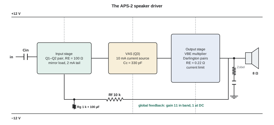
The architecture is the classic three-stage discrete power amplifier, the same plan as the op amp of lesson 4, but with a power output stage. The input stage is a differential pair, Q1 and Q2, with a 2 mA tail current from a current source and a current-mirror load; 100 Ω emitter resistors degenerate it to widen its linear range and to raise its slew rate for a given bandwidth (lesson 4). The voltage-amplifier stage (VAS) is a common-emitter transistor running at 10 mA from a current-source load, with the compensation capacitor C_c from its collector to its base. The output stage is a complementary class AB pair of power transistors with driver transistors, 0.22 Ω emitter resistors and a V_BE multiplier on the heat sink (lesson 10). Global feedback from the output through R_f = 10 kΩ to the inverting input, with R_g = 1 kΩ to ground through a 100 µF capacitor, sets the gain at 11 for audio but 1 at DC, so that the input stage's offset is not amplified.
Stage design
The input stage sets the amplifier's offset, noise, slew rate and unity-gain frequency. With 1 mA per side, each transistor has g_m = 38.7 mS; the 100 Ω emitter resistors reduce the stage's effective transconductance to g_m/(1 + g_m R_E) ≈ 7.95 mS and widen its linear input range from about ±50 mV to roughly ±200 mV. The current mirror converts the differential current into a single-ended output current with the full transconductance (lesson 3). The tail is a current source rather than a resistor, giving good rejection of the ±12 V rails' ripple, which appears as a common-mode disturbance.
The VAS converts that current into the large voltage swing needed to drive the output stage, about ±11 V, and the compensation capacitor across it creates the dominant pole by the Miller effect (lessons 4 and 8). Because the VAS must also supply the output stage's driver base currents and charge C_c, its current source is set at 10 mA, generous enough that the VAS never runs short of current at the highest frequencies and amplitudes the amplifier must handle.
The output stage uses complementary Darlington pairs, so the VAS sees the 8 Ω load multiplied by the product of two current gains, thousands of ohms, and the V_BE multiplier spans four base-emitter junctions. Amara sets the multiplier for a quiescent current of 30 mA, giving about 6.6 mV across each 0.22 Ω emitter resistor at rest, and mounts the multiplier transistor on the heat sink beside the output transistors. A current limiter on each side senses the emitter-resistor voltage and limits the output current to about 2.7 A, protecting the stage against a shorted speaker line.
Worked problem
Unity-gain frequency, crossover and slew rate
Choose C_c so that the loop crossover at the closed-loop gain of 11 lies comfortably below the output stage's pole, which Amara estimates at 2 MHz for the chosen power transistors, giving at least 60° of phase margin even if that pole drops to 1 MHz at high current. Then check the slew rate.
Show solution
- \[g_{m,eff} = \frac{38.7\ \text{mS}}{1 + 0.0387 \times 100} \approx 7.95\ \text{mS}\]
- Try C_c = 330 pF:
- \[f_u = \frac{7.95\times10^{-3}}{2\pi \times 330\ \text{pF}} \approx 3.8\ \text{MHz} \qquad f_c \approx \frac{f_u}{11} \approx 349\ \text{kHz}\]
- \[\text{PM} \approx 90 - \arctan\frac{0.349}{2} - \arctan\frac{0.349}{10} \approx 78^\circ \;(\text{about } 69^\circ \text{ if the pole falls to } 1\ \text{MHz})\]
- \[SR = \frac{2\ \text{mA}}{330\ \text{pF}} \approx 6.1\ \text{V}/\mu\text{s} \qquad \text{needed at 10 kHz, 10.5 V peak: } 2\pi \times 10^{4} \times 10.5 \approx 0.66\ \text{V}/\mu\text{s}\]
Answer: With C_c = 330 pF, the loop crosses over near 350 kHz with about 78° of phase margin, and keeps nearly 70° if the output stage's pole falls to 1 MHz. The slew rate of about 6 V/µs is nine times what a full-amplitude 10 kHz sine needs. A smaller C_c would give more loop gain for reducing distortion but less margin; 330 pF is Amara's balance, to be confirmed by simulation and by a step test on the bench.
Verifying the loop
The first verification is the loop gain and closed-loop response. The code models the forward path with the dominant pole set by C_c, the output stage's pole and a second, higher pole in the input stage, computes the phase margin and the loop gain at the audio frequencies of interest, and then the closed-loop gain across the specified band, including the input coupling capacitor and the feedback network's DC-blocking capacitor.
import cmath, math
fu, p2, p3 = 3.83e6, 2.0e6, 10e6          # unity-gain frequency of the forward path; non-dominant poles
A0 = 2e5                                  # low-frequency forward gain (sets the dominant pole)
fp1 = fu / A0
Rf, Rg, Cg = 10e3, 1e3, 100e-6            # feedback network with DC-blocking capacitor
Rin, Cin = 10e3, 220e-9                   # input coupling
def A(f):
    s = 1j * f
    return A0 / ((1 + s / fp1) * (1 + s / p2) * (1 + s / p3))
def beta(f):
    zg = Rg + 1 / (2j * math.pi * f * Cg)
    return zg / (zg + Rf)
def closed(f):
    hp = (2j * math.pi * f * Rin * Cin) / (1 + 2j * math.pi * f * Rin * Cin)
    return hp * A(f) / (1 + A(f) * beta(f))
lo, hi = 1e3, 1e8                         # crossover where |T| = 1
for _ in range(200):
    m = math.sqrt(lo * hi)
    if abs(A(m) * beta(m)) > 1: lo = m
    else: hi = m
pm = 180 + math.degrees(cmath.phase(A(m) * beta(m)))
print(f"crossover {m/1e3:.0f} kHz, phase margin {pm:.1f} deg")
for p in (1.0e6, 0.5e6):                  # sensitivity: what if the output-stage pole is lower?
    T = lambda f: A0 / ((1 + 1j*f/fp1) * (1 + 1j*f/p) * (1 + 1j*f/p3)) * beta(f)
    lo, hi = 1e3, 1e8
    for _ in range(200):
        x = math.sqrt(lo * hi)
        if abs(T(x)) > 1: lo = x
        else: hi = x
    print(f"  output pole {p/1e6:.1f} MHz: phase margin {180 + math.degrees(cmath.phase(T(x))):.1f} deg")
for f in (1e3, 10e3):
    print(f"loop gain at {f/1e3:4.0f} kHz: {abs(A(f)*beta(f)):6.1f} ({20*math.log10(abs(A(f)*beta(f))):.1f} dB)")
g1k = abs(closed(1e3))
for f in (100, 200, 1e3, 5e3, 10e3, 20e3):
print(f"closed-loop gain at {f:7.0f} Hz: {abs(closed(f)):6.3f} ({20*math.log10(abs(closed(f))/g1k):+.2f} dB re 1 kHz)")crossover 343 kHz, phase margin 78.3 deg output pole 1.0 MHz: phase margin 69.8 deg output pole 0.5 MHz: phase margin 57.4 deg loop gain at 1 kHz: 348.1 (50.8 dB) loop gain at 10 kHz: 34.8 (30.8 dB) closed-loop gain at 100 Hz: 8.911 (-1.81 dB re 1 kHz) closed-loop gain at 200 Hz: 10.343 (-0.51 dB re 1 kHz) closed-loop gain at 1000 Hz: 10.971 (+0.00 dB re 1 kHz) closed-loop gain at 5000 Hz: 10.998 (+0.02 dB re 1 kHz) closed-loop gain at 10000 Hz: 10.997 (+0.02 dB re 1 kHz) closed-loop gain at 20000 Hz: 10.989 (+0.01 dB re 1 kHz)
The model gives a crossover near 350 kHz and a phase margin close to the hand estimate, and the margin stays above 60° with the output pole at 1 MHz, falling below it only if the pole drops to 0.5 MHz, which would need a far slower output transistor than the ones chosen. The loop gain is about 350, or 51 dB, at 1 kHz and about 35 at 10 kHz, so output-stage distortion is reduced by those factors. The closed-loop response is flat within a few hundredths of a decibel from 1 kHz to 20 kHz and only about 0.5 dB down at 200 Hz, inside the ±1 dB requirement. That small droop comes from the low corner set by the 220 nF input capacitor and the 10 kΩ input resistor, near 72 Hz, chosen to keep useless bass out of the small speaker while leaving the voice band intact.
Verifying distortion
The second verification is distortion. The output stage's transfer curve is computed from the exponential laws of its two transistors with their emitter resistors and bias voltage, for a class B bias (no quiescent current) and for the chosen 30 mA class AB bias. The code finds each stage's distortion on its own, driven to a small and a full output, and then inside the feedback loop using the loop gains just found at 1 kHz and 10 kHz.
import math
VT, IS, RE, RL = 0.02585, 1e-12, 0.22, 8.0
def vbias_for(IQ):
    return 2 * VT * math.log(IQ / IS) + 2 * IQ * RE if IQ > 0 else 0.0
def drive_for(vo, vb):
    """Base drive (relative to mid-bias) that produces output vo, for bias voltage vb."""
    iL = vo / RL
    lo, hi = max(iL, 0.0) + 1e-15, abs(iL) + 5.0     # npn current; pnp current = in - iL
    for _ in range(200):
        i_n = (lo + hi) / 2
        i_p = i_n - iL
        if i_p <= 0: lo = i_n; continue
        f = VT * math.log(i_n / IS) + VT * math.log(i_p / IS) + (i_n + i_p) * RE - vb
        if f > 0: hi = i_n
        else: lo = i_n
    return vo + VT * math.log(i_n / IS) + i_n * RE - vb / 2
grid = [-11 + 22 * k / 2200 for k in range(2201)]
def tables(IQ):
    vb = vbias_for(IQ)
    return [drive_for(v, vb) for v in grid]
def interp(xs, ys, x):
    lo, hi = 0, len(xs) - 1
    while hi - lo > 1:
        mid = (lo + hi) // 2
        if xs[mid] > x: hi = mid
        else: lo = mid
    t = (x - xs[lo]) / (xs[hi] - xs[lo])
    return ys[lo] + t * (ys[hi] - ys[lo])
N = 256
def thd(out):
    h = []
    for k in range(1, 10):
        re = sum(out[n] * math.cos(2 * math.pi * k * n / N) for n in range(N))
        im = sum(out[n] * math.sin(2 * math.pi * k * n / N) for n in range(N))
        h.append(math.hypot(re, im))
    return 100 * math.sqrt(sum(x * x for x in h[1:])) / h[0]
beta = 1 / 11
for name, IQ in (("class B ", 0.0), ("class AB", 0.030)):
    drv = tables(IQ)
    for Vpk in (0.5, 8.0):
        # open loop: drive the stage with a sine sized for the target output peak
        a = interp(grid, drv, Vpk)
        ol = [interp(drv, grid, a * math.sin(2 * math.pi * n / N)) for n in range(N)]
        res = [f"{name} {Vpk:3.1f} V peak: open loop {thd(ol):7.4f} %"]
        for f, T in (("1 kHz", 350.0), ("10 kHz", 35.0)):
            Af = T / beta                 # forward gain from error to output-stage drive
            xs = [d / Af + beta * v for d, v in zip(drv, grid)]   # input needed for each output
            amp = interp(grid, xs, Vpk)
            cl = [interp(xs, grid, amp * math.sin(2 * math.pi * n / N)) for n in range(N)]
            res.append(f"{f} {thd(cl):7.4f} %")
print(", ".join(res))class B 0.5 V peak: open loop 24.5089 %, 1 kHz 0.1204 %, 10 kHz 1.1598 % class B 8.0 V peak: open loop 2.8604 %, 1 kHz 0.0085 %, 10 kHz 0.0830 % class AB 0.5 V peak: open loop 0.0681 %, 1 kHz 0.0002 %, 10 kHz 0.0020 % class AB 8.0 V peak: open loop 0.2404 %, 1 kHz 0.0007 %, 10 kHz 0.0069 %
The results show why both class AB bias and feedback are needed. Open loop, the class B stage produces gross distortion at 0.5 V peak, because a dead zone of more than a volt swallows most of the small signal; even feedback with a loop gain of 350 leaves measurable crossover distortion at low level, and at 10 kHz, with a loop gain of 35, it is far worse. The class AB stage starts with far lower open-loop distortion, below 0.1 percent at low level and a few tenths of a percent at full output, and feedback then brings it to about a thousandth of a percent or less at 1 kHz and below 0.01 percent at 10 kHz, at both the quiet and the rated output. The specification's 0.5 percent at 1 kHz and 1 percent at 10 kHz are met with wide margin. The model ignores the drivers, the VAS's own nonlinearity and the speaker's reactive load, so the bench result will be higher, but the ranking and the order of magnitude are what the design review needs.
Offset, thermal design and protection
The DC offset at the output comes from the input stage alone, because the 100 µF capacitor makes the DC gain 1. The input pair's bias current is about 1 mA/(β + 1) ≈ 10 µA for β = 100; if it flowed through unequal resistances at the two bases it would create a large offset, so Amara makes the input resistor equal to R_f, 10 kΩ, leaving only the offset current, perhaps 1 µA, times 10 kΩ, about 10 mV, plus the pair's own V_OS of a few millivolts. The total, below 20 mV worst case, meets the 50 mV requirement without trimming.
Worked problem
Heat sink and junction temperature check
From lesson 10, the worst-case dissipation is 1.82 W per output transistor (3.65 W total) at V_p = 7.6 V. Add the quiescent dissipation, 2 × 12 V × 30 mA = 0.72 W, conservatively, and find the heat sink and junction temperatures in the 74 °C housing with the 10 °C/W heat sink, θ_JC = 3.0 °C/W and θ_CS = 0.5 °C/W.
Show solution
- \[P_{total} \approx 3.65 + 0.72 \approx 4.37\ \text{W} \qquad T_S = 74 + 4.37 \times 10 \approx 118\ ^\circ\text{C}\]
- \[T_J = 118 + \frac{4.37}{2} \times 3.5 \approx 126\ ^\circ\text{C}\]
Answer: Adding the quiescent dissipation on top of the worst-case signal dissipation is pessimistic, because the quiescent current is part of the class AB stage's current rather than an extra load at full signal, but even this conservative estimate puts the junctions at about 126 °C, right at Amara's working limit and well below the 150 °C absolute rating. With the realistic estimate of lesson 10, about 3.65 W, the heat sink runs near 111 °C and the junctions near 117 °C. Amara keeps the 10 °C/W sink and adds a thermostat on the heat sink that tells the microcontroller to reduce the volume by 6 dB if the sink exceeds 115 °C, an inexpensive safeguard against a stuck tone on a heat-wave afternoon.
Protection completes the design. The current limiters hold the output current below about 2.7 A into a short. A Zobel network of 10 Ω and 100 nF across the output keeps the load resistive at high frequencies, where the speaker and its cable would otherwise look inductive and capacitive and erode the phase margin, and a small air-core inductor with a parallel damping resistor isolates the loop from long speaker cables. A DC-detection circuit compares the low-pass-filtered output with ±1 V and opens a relay in series with the speaker if a fault drives the output toward a rail, so a failed transistor cannot burn the voice coil. At switch-on, the relay closes only after the rails and the feedback capacitor have settled, avoiding a loud thump from the speaker in a quiet residential street at night.
Bench testing and the design review
Leo builds three prototypes and tests them against every line of the specification, at room temperature and in the environmental chamber at −40 °C and +74 °C. The test plan includes the DC operating points of every stage against Amara's calculations; the quiescent current at 25 °C and with the heat sink at 110 °C; the gain and frequency response from 100 Hz to 50 kHz; THD at 0.5 W and 4 W at 1 kHz and 10 kHz with an audio analyzer; a small-signal square-wave test into the real speaker and 15 m of cable, with and without the Zobel network, to read overshoot as phase margin (lesson 8); slew rate with a large square wave; a short-circuit test at full drive; the DC fault test with a deliberately shorted output transistor on a spare board; and a continuous worst-case tone in the 74 °C chamber, with the heat sink and transistor case temperatures logged until they stabilize.
The results mostly agree with the calculations. The quiescent current is 32 mA at room temperature and 37 mA with the heat sink at 110 °C, confirming that the thermal tracking works, though not perfectly. THD at 4 W and 1 kHz is 0.015 percent, higher than the simulation's thousandth of a percent because of the drivers and VAS, but thirty times below the requirement. The square-wave test into the speaker and cable shows about 6 percent overshoot without the Zobel network and less than 2 percent with it. In the 74 °C chamber the heat sink stabilizes at 108 °C with the worst-case tone. One result surprises everyone: at −40 °C the amplifier's quiescent current falls to 18 mA and the crossover distortion at 0.5 W rises to 0.08 percent, still within specification but four times the room-temperature value. Amara traces it to the thermal tracking working in reverse and adjusts the multiplier ratio slightly, accepting a few more milliamps at the hot end.
At the design review, Daniel walks the team through each specification line, the calculation that predicted it, the simulation that checked it and the measurement that confirmed it, and records every discrepancy with its explanation. He also asks for the class D comparison from lesson 11 to be kept in the design file, so the next housing revision can revisit the choice. When the review closes, Daniel signs the design package as the professional engineer responsible, and the APS-2 moves to compliance testing and a field trial at two Madison intersections. For Amara, who will sit the PE exam once she has her required experience, the review record is also evidence of exactly the kind of engineering work the license requires.
Common mistakes
MistakeChoosing C_c by copying another design.
InsteadCompute the unity-gain frequency, the crossover at the closed-loop gain, and the phase margin with the real output-stage pole.
MistakeTesting stability with a resistive dummy load only.
InsteadTest with the real speaker and cable; reactive loads change the margin.
MistakeLeaving the input and feedback resistances unequal.
InsteadBias current through unequal resistances creates offset; equalize them or use DC gain 1.
MistakeChecking distortion only at full power.
InsteadCrossover distortion is worst at low levels; test both, and at temperature extremes.
Summary and key terms
- A design project runs from specification through architecture, stage design, verification and bench test to a design review.
- The speaker driver uses a degenerated differential input stage, a Miller-compensated VAS and a class AB output stage in one feedback loop.
- Degeneration lowers g_m,eff to about 7.95 mS; with C_c = 330 pF, f_u ≈ 3.8 MHz and the loop crosses over near 350 kHz.
- Phase margin near 78°, falling to about 69° if the output pole halves, meets the 60° requirement.
- Loop gains of about 350 at 1 kHz and 35 at 10 kHz reduce class AB distortion to small fractions of a percent.
- DC gain of 1 and equal input and feedback resistances keep offset below 20 mV.
- Thermal design, current limiting, a Zobel network and DC protection make the amplifier survive the field.
- Voltage-amplifier stage
- The high-gain middle stage of a power amplifier, which provides the large voltage swing that drives the output stage.
- Global feedback
- Feedback taken from the final output back to the input of the whole amplifier.
- Design review
- A structured check of a design against its specification, calculations, simulations and measurements before it is released.
- DC protection
- A circuit that disconnects a loudspeaker if a fault puts DC on the amplifier output.
- Quiescent current
- The current through an output stage with no signal, set by its bias.
- Specification
- The measurable requirements a design must meet, with the reason for each.
Practice problems
Work each problem on paper first, then reveal the answer to check.
With R_f = 10 kΩ and R_g = 1 kΩ, what is the closed-loop gain? What is the DC gain if R_g has a series capacitor?
Show answer
11; 1 at DC, because the capacitor blocks DC in the ground leg.
Find g_m,eff of a pair at 0.5 mA per side with 220 Ω emitter resistors.
Show answer
g_m = 19.3 mS; 19.3 m/(1 + 4.25) ≈ 3.7 mS.
With g_m,eff = 3.7 mS, what C_c gives f_u = 2 MHz?
Show answer
3.7 m/(2π × 2 MHz) ≈ 294 pF.
A 15 kΩ input resistor and a 10 kΩ feedback resistor carry 8 µA of bias current. Estimate the offset they create.
Show answer
5 kΩ × 8 µA = 40 mV.
The heat sink is 8 °C/W and the stage dissipates 3.65 W in 74 °C air. Find the heat sink temperature.
Show answer
74 + 29.2 ≈ 103 °C.
Why is a small-signal square-wave test into the real speaker part of the test plan?
Show answer
Its overshoot reveals the phase margin with the actual reactive load.
Lesson quiz · 5 questions
Score 60% or more to complete this lesson.
Create a free account to save your progress, take quizzes and earn a certificate.