
ELE-340 · Lesson 10 of 12 · 25 min
Output stages and thermal design
The last stage of a power amplifier has a different job from the stages before it. It must deliver real power, watts rather than milliwatts, into a low-impedance load such as a loudspeaker, a motor winding or a cable, with low distortion, without wasting so much power that it overheats, and without destroying itself when the load is shorted. Voltage gain is unimportant; most output stages are followers with a gain just under 1. What matters are the current capability, the efficiency, the linearity near zero crossing and the temperature of the transistors. This lesson compares class A, B and AB output stages, derives their efficiency and worst-case dissipation, shows how class AB is biased and why that bias can run away thermally, and finishes with heat-sink design.
The APS-2's loudspeaker is a weatherproof 8 Ω driver that must produce up to 4 W, enough for the locator tone and voice messages to be heard over heavy traffic. The station's power amplifier runs from ±12 V rails derived from the controller's supply, and it sits in a sealed aluminum housing on a pole where, on a summer afternoon in full sun, the air inside can reach 74 °C. Amara's output stage has to work there for twenty years.
Class A: the simple follower
A class A output stage conducts for the whole signal cycle. The simplest form is an emitter follower biased by a current source I_Q, with the load connected to the emitter. To drive a peak load current I_p in both directions, the transistor must carry at least I_Q = I_p at rest, so it can fall to zero current at the negative peak and rise to 2I_Q at the positive peak. The current flows whether or not there is signal, so the supply power is constant, and most of it heats the transistor and the current source. For a follower on ±V_CC rails with a current-source bias, the efficiency is
For the APS-2 at 4 W into 8 Ω, the peak current is 1 A, so I_Q = 1 A and the stage draws 2 × 12 V × 1 A = 24 W all the time, with only 4 W reaching the speaker at full output and nothing at all reaching it while the station waits silently between pushes. A class A design is the most linear output stage, and audio enthusiasts still build them, but in a sealed pole housing it is out of the question.
Class B: the complementary push-pull stage
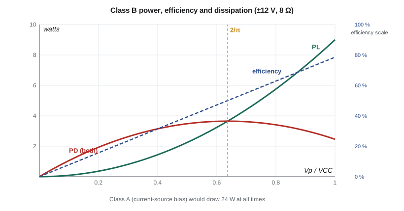
A class B stage uses two complementary emitter followers: an npn transistor from the positive rail that conducts on positive half-cycles and a pnp transistor from the negative rail that conducts on negative half-cycles. With their bases driven together and their emitters joined at the output, each transistor is off at rest and conducts for half the cycle. No current flows without signal, so the stage wastes no power at idle, and at full output it is far more efficient than class A. For a sine of peak V_p into R_L, each rail supplies a half-wave current whose average is I_p/π, and
The dissipation P_D = P_S − P_L is not largest at full output. Differentiating shows that it peaks at V_p = 2V_CC/π, about 64 percent of the rail, where
Worked problem
Dissipation of the APS-2 class B stage
The stage runs from ±12 V into 8 Ω. Find the maximum transistor dissipation, and the efficiency and dissipation at the rated 4 W (V_p = 8 V).
Show solution
- \[P_{D,max} = \frac{2 \times 12^2}{\pi^2 \times 8} \approx 3.65\ \text{W total} \;(1.82\ \text{W per transistor, at } V_p = 7.6\ \text{V})\]
- \[P_S = \frac{2 \times 12 \times 8}{\pi \times 8} \approx 7.64\ \text{W} \qquad P_L = \frac{8^2}{16} = 4.0\ \text{W}\]
- \[\eta = \frac{4.0}{7.64} \approx 52\ \% \qquad P_D \approx 3.64\ \text{W}\]
Answer: At 4 W, the stage is about 52 percent efficient and dissipates 3.64 W, essentially the worst case, because 8 V is close to 2V_CC/π = 7.6 V. Running the rails lower, say ±10 V, would raise efficiency at 4 W but leave little headroom for the drop across the transistors, so Amara keeps ±12 V and designs the heat sink for 1.82 W per transistor.
Crossover distortion and class AB
A pure class B stage has a flaw. Neither transistor conducts until its base–emitter voltage reaches about 0.6 V, so for input voltages between −0.6 V and +0.6 V the output stays near zero: a dead zone appears at every zero crossing. The resulting crossover distortion is worst at low volume, where the dead zone is a large fraction of the signal, and it sounds harsh because it produces high-order harmonics. Feedback reduces it but cannot remove it, because inside the dead zone the stage's gain, and therefore the loop gain, collapses.
Class AB removes the dead zone by biasing both transistors slightly on at rest, so that each conducts for a little more than half the cycle and the two overlap around zero. The bias is a voltage of about 2V_BE between the two bases, made by two diodes in series or, more adjustably, by a V_BE multiplier: a transistor with resistor R_1 from collector to base and R_2 from base to emitter, whose collector-to-emitter voltage is
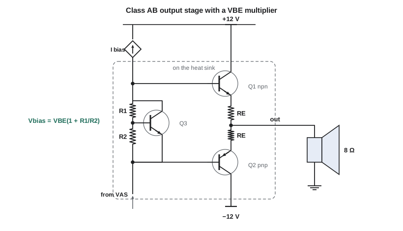
The small emitter resistors R_E, typically 0.1 to 0.47 Ω, help set the quiescent current I_Q and share current between paralleled transistors. The quiescent current is usually tens of milliamps: enough to keep both devices conducting around zero, but a tiny dissipation compared with the class A stage. With 0.22 Ω emitter resistors, designers often aim for roughly 25 mV across each, which happens to minimize the variation in the stage's output resistance through the crossover region.
Thermal runaway
Class AB bias has a hazard. At a fixed base-to-base voltage, a transistor's current rises as it warms, because V_BE for a given current falls about 2 mV/°C. More current means more dissipation, more heat and still more current. If the bias voltage does not fall to match, the loop can run away until the transistors fail. The defenses are the emitter resistors, which add a voltage that rises with current, and above all thermal tracking: the V_BE multiplier transistor is mounted on the output transistors' heat sink, so its own V_BE, and therefore V_bias, falls as the heat sink warms. The code below compares a fixed bias with a tracking bias as the heat sink warms from 25 °C to 100 °C.
import math
VT0, k_vbe = 0.02585, -0.002            # V_BE tempco about -2 mV/degC
RE, IQ0, T0 = 0.22, 0.030, 25.0          # emitter resistors, design quiescent current at 25 degC
def iq(T, tracking):
    """Solve 2*VBE(I,T) + 2*I*RE = Vbias(T) for the quiescent current I."""
    vbe0 = 0.65                          # V_BE at IQ0 and 25 degC
    vbias = 2 * vbe0 + 2 * IQ0 * RE
    if tracking:                          # multiplier on the heat sink: Vbias tracks 2*VBE
        vbias += 2 * k_vbe * (T - T0)
    lo, hi = 1e-4, 5.0
    for _ in range(80):
        I = math.sqrt(lo * hi)
        vbe = vbe0 + VT0 * math.log(I / IQ0) + k_vbe * (T - T0)
        if 2 * vbe + 2 * I * RE > vbias: hi = I
        else: lo = I
    return I
print("heat sink   fixed bias   tracking bias")
for T in (25, 50, 75, 100):
    print(f"{T:6.0f} C   {iq(T, False)*1e3:8.0f} mA   {iq(T, True)*1e3:8.1f} mA")
# Class B dissipation and efficiency for +/-12 V into 8 ohms
VCC, RL = 12.0, 8.0
for Vp in (2.0, 4.0, 2 * VCC / math.pi, 8.0, 10.5):
    PL = Vp ** 2 / (2 * RL); PS = 2 * VCC * Vp / (math.pi * RL)
print(f"Vp = {Vp:5.2f} V: PL = {PL:4.2f} W, PS = {PS:4.2f} W, PD = {PS-PL:4.2f} W, eff = {100*PL/PS:4.1f} %")heat sink fixed bias tracking bias
25 C 30 mA 30.0 mA
50 C 107 mA 30.0 mA
75 C 240 mA 30.0 mA
100 C 406 mA 30.0 mA
Vp = 2.00 V: PL = 0.25 W, PS = 1.91 W, PD = 1.66 W, eff = 13.1 %
Vp = 4.00 V: PL = 1.00 W, PS = 3.82 W, PD = 2.82 W, eff = 26.2 %
Vp = 7.64 V: PL = 3.65 W, PS = 7.30 W, PD = 3.65 W, eff = 50.0 %
Vp = 8.00 V: PL = 4.00 W, PS = 7.64 W, PD = 3.64 W, eff = 52.4 %
Vp = 10.50 V: PL = 6.89 W, PS = 10.03 W, PD = 3.14 W, eff = 68.7 %With a fixed bias, the quiescent current climbs from 30 mA at 25 °C to several hundred milliamps at 100 °C, adding watts of dissipation that heat the transistors further: the start of thermal runaway. With the V_BE multiplier tracking the heat sink, the current stays at 30 mA in this idealized model. Real tracking is imperfect, because the output transistors' junctions run hotter than the heat sink and the multiplier senses the sink, not the junctions, so designers set the multiplier ratio slightly above the ideal or add more emitter resistance, and they check the quiescent current at the hottest expected heat-sink temperature.
Driving the output stage
A power transistor's β at amperes of collector current may be only 30 to 80, so a 1 A peak output current needs 15 to 35 mA of base current, more than an op amp or a small-signal stage can supply cleanly. Output stages therefore add drivers: a complementary Darlington pair on each side, giving β₁β₂, or a Sziklai (complementary feedback) pair, which behaves like a single high-β transistor with only one V_BE of offset. The bias voltage must then cover four junctions in the Darlington case. Power MOSFET output stages avoid base current altogether but need a few volts of gate drive and present large gate capacitances that the driver must charge quickly. Either way, the stage before the output must deliver current, not just voltage, at the highest audio frequency.
Protection and safe operating area
A power transistor can fail in several ways besides overheating: by exceeding its maximum collector current, its maximum voltage, or its safe operating area (SOA), the region of simultaneous voltage and current it can survive, which for bipolar transistors is restricted at high voltage by second breakdown, a localized hot spot that destroys the junction. A short circuit across the output is the classic hazard: the output transistor then sees the full rail voltage at a large current. Output stages therefore include current limiting, usually a small transistor that senses the voltage across R_E and steals base drive when it exceeds about 0.6 V, so with R_E = 0.22 Ω the limit is near 2.7 A. More elaborate V-I limiters reduce the allowed current when the transistor's voltage is high, keeping the stage inside its SOA. A loudspeaker also needs protection from DC: a fault that sends the output to a rail would burn the voice coil, so many amplifiers add a relay or fuse that disconnects the speaker if DC appears at the output.
Thermal design and heat sinks
Heat flows from the transistor's junction to its case, from the case through an insulating pad to the heat sink, and from the sink to the surrounding air. Each step has a thermal resistance in °C/W, and they add like series resistors:
θ_JC comes from the transistor datasheet, about 1 to 4 °C/W for power transistors in TO-220 and TO-247 packages; θ_CS depends on the interface, about 0.2 to 1 °C/W with thermal grease or a pad; θ_SA comes from the heat sink datasheet and falls with the sink's size and with airflow. The datasheet's maximum junction temperature, often 150 °C, is an absolute limit; reliability falls steeply as it is approached, so designers set a lower working limit, often 110 to 125 °C, and design for the worst ambient temperature and the worst-case dissipation, not the typical one.
Worked problem
Choosing the APS-2 heat sink
Each output transistor dissipates up to 1.82 W, the housing air reaches 74 °C, and Amara sets a working limit of T_J = 125 °C. Each transistor has θ_JC = 3.0 °C/W and θ_CS = 0.5 °C/W with an insulating pad. Both transistors share one heat sink. Find the required θ_SA.
Show solution
- Allowed rise from heat sink to junction for each transistor:
- \[T_S \le 125 - 1.82 \times (3.0 + 0.5) \approx 118.6\ ^\circ\text{C}\]
- The sink carries both transistors' heat:
- \[\theta_{SA} \le \frac{118.6 - 74}{3.65} \approx 12.2\ ^\circ\text{C/W}\]
Answer: A heat sink of about 12 °C/W or better meets the limit at the worst-case sine-wave dissipation. Amara chooses a 10 °C/W extrusion, which gives a margin of about 7 °C, and bolts it to the housing wall so that the housing itself spreads heat. Real speech and the short locator tick dissipate far less on average than a continuous sine at 7.6 V peak, but a continuous tone during a maintenance test would hit the worst case, so she designs for it.
Thermal time constants also matter. A heat sink takes minutes to warm up, while a junction responds in milliseconds; datasheets give transient thermal impedance curves showing that short pulses of power can exceed the steady-state rating. For audio, where peaks are short and the average is low, this gives extra margin; for a stuck tone or a shorted output, only the steady-state calculation is safe.
Common mistakes
MistakeDesigning the heat sink for the dissipation at full output power.
InsteadIn class B the worst dissipation is at V_p = 2V_CC/π, about 64 percent of the rail.
MistakeBiasing a class AB stage with a fixed voltage that does not track temperature.
InsteadMount the V_BE multiplier on the heat sink and use emitter resistors to prevent thermal runaway.
MistakeUsing the typical ambient temperature in thermal calculations.
InsteadUse the worst case, such as a sealed housing in summer sun.
MistakeRunning junctions at the absolute maximum rating.
InsteadSet a working limit well below it; reliability falls steeply at high temperature.
Summary and key terms
- Class A conducts all the time; its efficiency is at most 25 percent and it dissipates heavily at idle.
- Class B uses complementary followers, each conducting half the cycle; η = (π/4)(V_p/V_CC) ≤ 78.5 percent.
- Class B dissipation peaks at V_p = 2V_CC/π, with P_D,max = 2V_CC²/(π²R_L) for both transistors.
- Crossover distortion comes from the ±0.6 V dead zone; class AB biasing with diodes or a V_BE multiplier removes it.
- Thermal runaway is prevented by emitter resistors and a bias generator that tracks heat-sink temperature.
- Drivers (Darlington or Sziklai pairs) supply the base current; current limiting and SOA protection prevent failure.
- T_J = T_A + P_D(θ_JC + θ_CS + θ_SA); design for the worst ambient and the worst dissipation.
- Class A
- An output stage in which the transistors conduct over the whole signal cycle.
- Class B
- An output stage in which each of two transistors conducts for half of the cycle and neither conducts at rest.
- Class AB
- A push-pull stage biased so that both transistors conduct slightly at rest, removing crossover distortion.
- Crossover distortion
- Distortion near zero crossings caused by the dead zone of an unbiased push-pull stage.
- V_BE multiplier
- A transistor and two resistors that produce a bias voltage of V_BE(1 + R₁/R₂).
- Thermal runaway
- A destructive cycle in which rising temperature raises current, which raises temperature further.
- Thermal resistance
- The temperature rise per watt of heat flow across a part of the heat path, in °C/W.
Practice problems
Work each problem on paper first, then reveal the answer to check.
A class B stage on ±15 V drives 4 Ω. Find the maximum total transistor dissipation.
Show answer
2 × 225/(π² × 4) ≈ 11.4 W.
At what output amplitude does that maximum occur?
Show answer
2 × 15/π ≈ 9.5 V peak.
Find the efficiency of a class B stage delivering V_p = 9 V from ±12 V rails.
Show answer
(π/4)(9/12) ≈ 59 percent.
A V_BE multiplier uses R₁ = 1.5 kΩ and R₂ = 1 kΩ with V_BE = 0.62 V. Find V_bias.
Show answer
0.62 × 2.5 = 1.55 V.
A transistor dissipates 5 W with θ_JC = 1.5, θ_CS = 0.5 and θ_SA = 6 °C/W at T_A = 40 °C. Find T_J.
Show answer
40 + 5 × 8 = 80 °C.
Why does a class A follower driving 1 A peak need a quiescent current of at least 1 A?
Show answer
The transistor must stay conducting at the negative peak, when the load draws current away from it.
Lesson quiz · 5 questions
Score 60% or more to complete this lesson.
Create a free account to save your progress, take quizzes and earn a certificate.