
ELE-340 · Lesson 1 of 12 · 25 min
Multistage amplifiers and coupling
A single transistor stage can give gain, or a high input resistance, or a low output resistance, but rarely all three at once, and never with the precision, bandwidth and output power that real products need. Practical amplifiers are therefore built from several stages in a chain, each chosen for one job: an input stage that accepts the signal without loading the source and rejects interference, gain stages that provide most of the amplification, and an output stage that delivers current to the load. Electronics I analyzed each stage on its own. Electronics II is about how stages work together: how they load one another, how they are coupled, how a differential input rejects noise, how feedback makes the whole chain precise, how it stays stable at high frequencies, how oscillators deliberately make it unstable, and how an output stage can push watts into a loudspeaker without overheating.
The course follows one product at Cedarline Controls in Madison, Wisconsin. Amara Osei, now in her second year as an engineer intern, has been given the analog design of the APS-2, the company's next accessible pedestrian signal push-button station. Daniel Fortin, PE, the senior hardware designer, reviews her work, and Leo Tremblay, a co-op student, builds and measures prototypes on the bench. The APS-2 listens to street noise through a remote microphone on the pole, and drives a weatherproof 8 Ω loudspeaker with a locator tone and spoken messages whose loudness tracks the ambient noise, so a pedestrian who is blind or has low vision can find the button and know when the walk interval begins.
The APS-2 signal chain
The signal chain has two halves. On the listening side, the remote microphone sits about 15 m away at the top of the pole, so its signal travels down a long cable that also picks up hum from the 60 Hz street-lighting circuits. A differential receiver (lesson 3) rejects that hum, and a preamplifier based on the noise-sensing amplifier from Electronics I brings the signal up to a level the microcontroller's analog-to-digital converter can measure. On the talking side, the microcontroller generates the 880 Hz locator tick and the voice messages, a digitally controlled attenuator sets the volume, and a power amplifier (lessons 10 to 12) drives the loudspeaker with up to 4 W. Every block in that chain is a multistage amplifier or part of one.
Two-port models and loading
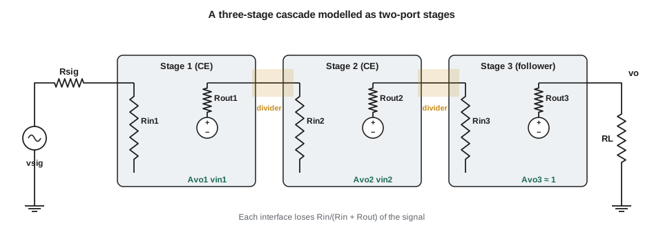
The cleanest way to analyze a cascade is to replace each stage by a two-port model: an input resistance R_in, an open-circuit voltage gain A_vo and an output resistance R_out. The model hides the transistor details and keeps only what matters to the neighbors. When stage k drives stage k + 1, its Thévenin output, A_vo,k v_in,k behind R_out,k, sees the input resistance of the next stage, so only the fraction R_in,k+1/(R_in,k+1 + R_out,k) of its open-circuit output reaches the next input. The overall gain is the product of every stage's open-circuit gain and every interface divider, including the one at the source and the one at the load:
Two habits follow from the formula. First, each divider should be close to 1: a stage should have an output resistance much smaller than the next stage's input resistance, a condition designers call voltage bridging. Second, it is usually wrong to compute stage gains in isolation and multiply them, because the load on a stage changes its gain. Loading works the other way too: a stage's input resistance can depend on its load. For a CE stage with r_o neglected it does not, but for an emitter follower R_in ≈ (β + 1)(r_e + R_L'), so a heavy load lowers the input resistance and loads the stage before it.
Worked problem
Gain of the Electronics I microphone amplifier as a cascade
The noise-sensing amplifier from Electronics I has two degenerated common-emitter stages and an emitter follower. Modeled as two-ports: stage 1 has R_in = 12 kΩ, A_vo = −12 and R_out = 5.1 kΩ; stage 2 has R_in = 15 kΩ, A_vo = −12 and R_out = 5.1 kΩ; the follower has R_in = 150 kΩ, A_vo = 0.99 and R_out = 46 Ω. The microphone has R_sig = 2 kΩ and the envelope detector presents about R_L = 1 kΩ. Find the overall gain.
Show solution
- Source divider and first stage:
- \[\frac{12}{2 + 12} \times (-12) = 0.857 \times (-12) = -10.3\]
- First interface and second stage:
- \[\frac{15}{5.1 + 15} \times (-12) = 0.746 \times (-12) = -8.96\]
- Second interface, follower and load:
- \[\frac{150}{5.1 + 150} \times 0.99 \times \frac{1000}{46 + 1000} = 0.967 \times 0.99 \times 0.956 = 0.915\]
- \[\frac{v_o}{v_{sig}} = (-10.3)(-8.96)(0.915) \approx 84 \;(38.5\ \text{dB})\]
Answer: The overall gain is about 84, or 38.5 dB. Multiplying the open-circuit gains alone would have given 12 × 12 × 0.99 ≈ 143, so loading costs about 40 percent of the gain. The largest loss is at the first interface, where the 5.1 kΩ output of stage 1 drives only 15 kΩ.
import math
# Two-port cascade: each stage is (Rin, Avo, Rout). Units: ohms.
Rsig, RL = 2e3, 1e3
stages = [("CE 1", 12e3, -12.0, 5.1e3),
          ("CE 2", 15e3, -12.0, 5.1e3),
          ("follower", 150e3, 0.99, 46.0)]
def cascade(stages, Rsig, RL, verbose=False):
    gain, rprev = 1.0, Rsig
    for name, rin, avo, rout in stages:
        div = rin / (rin + rprev)
        gain *= div * avo
        if verbose:
            print(f"{name:9s} divider {div:5.3f}  stage gain {avo:+7.2f}  running gain {gain:+8.2f}")
        rprev = rout
    div = RL / (RL + rprev)
    gain *= div
    if verbose:
        print(f"{'load':9s} divider {div:5.3f}  overall gain {gain:+8.2f} ({20*math.log10(abs(gain)):.1f} dB)")
    return gain
g = cascade(stages, Rsig, RL, True)
naive = math.prod(s[2] for s in stages)
print(f"product of open-circuit gains: {naive:.0f}; loading loses {100*(1-g/naive):.0f} %")
# What if stage 1's collector resistor drove a follower before stage 2?
better = [stages[0], ("buffer", 150e3, 0.99, 46.0), stages[1], stages[2]]
print(f"with a buffer between the CE stages: {cascade(better, Rsig, RL):.0f}")CE 1 divider 0.857 stage gain -12.00 running gain -10.29 CE 2 divider 0.746 stage gain -12.00 running gain +92.11 follower divider 0.967 stage gain +0.99 running gain +88.19 load divider 0.956 overall gain +84.31 (38.5 dB) product of open-circuit gains: 143; loading loses 41 % with a buffer between the CE stages: 108
The last line of the output shows the price of a weak interface. A follower between the two CE stages lifts the gain from about 84 to about 108, because the 5.1 kΩ output of stage 1 then sees 150 kΩ instead of 15 kΩ. Whether the extra transistor is worth it is a design decision: here Amara would rather adjust the resistor values, because the noise-sensing channel needs only a known gain, not the largest possible one.
Ways to couple stages
Stages must pass the signal while keeping each transistor at its own bias point. There are four classic ways to connect them, each with its own trade-offs:
| Coupling | How it works | Strengths | Limitations |
|---|---|---|---|
| Capacitor (RC) | A series capacitor passes AC and blocks DC, so each stage is biased independently | Simple; each stage designed alone; DC drift does not accumulate | No response at DC; low-frequency corners add; large capacitors cannot be integrated |
| Direct (DC) | The output node of one stage is wired straight to the input of the next | Response down to DC; no large capacitors; standard inside integrated circuits | Bias points interact; DC offsets and drift are amplified by later stages |
| Transformer | A transformer passes AC and can match impedances or isolate grounds | Impedance matching; galvanic isolation; balanced signals | Bulky, costly, limited bandwidth, picks up magnetic fields |
| Optical | An LED and photodetector carry the signal across an isolation barrier | Complete galvanic isolation for safety or noise | Nonlinear and slow unless designed carefully |
Discrete audio and sensor circuits often use capacitor coupling, as the Electronics I microphone amplifier did. Integrated circuits use direct coupling almost exclusively, because a capacitor large enough to pass audio frequencies would occupy more silicon than hundreds of transistors. Once stages are direct-coupled, the designer must solve two problems that capacitor coupling hid: the DC level at each node must suit the next stage, and any DC error at the input is amplified along with the signal.
Direct coupling and level shifting
In a chain of npn common-emitter stages, each collector sits several volts above its base. Coupling collector to base directly would push every stage's bias point higher until the last stage saturated against the supply. Designers shift the DC level down between stages in several ways: by alternating npn and pnp stages, since a pnp stage's collector sits below its emitter; by an emitter follower, which drops one V_BE; by a Zener diode or a string of diodes in series with the signal path; or by a current source driving a resistor, which drops a fixed voltage without affecting the signal much. Op amps use these tricks so that the output can sit at 0 V when the input is at 0 V.
Worked problem
A complementary direct-coupled pair
Stage 1 is an npn CE stage on a 12 V supply with its collector at 7.0 V. Stage 2 is a pnp CE stage whose emitter connects through R_E2 to the 12 V supply and whose base connects directly to stage 1's collector. Stage 2 should run at I_C2 = 1 mA with V_EB = 0.65 V. Find R_E2, and the stage 2 collector resistor R_C2 to ground that puts its collector at 4.0 V.
Show solution
- The pnp emitter sits one V_EB above its base:
- \[V_{E2} = 7.0 + 0.65 = 7.65\ \text{V}\]
- \[R_{E2} = \frac{12 - 7.65}{1\ \text{mA}} = 4.35\ \text{k}\Omega \to 4.3\ \text{k}\Omega\]
- \[R_{C2} = \frac{4.0\ \text{V}}{1\ \text{mA}} = 4.0\ \text{k}\Omega \to 3.9\ \text{k}\Omega\]
Answer: With 4.3 kΩ and 3.9 kΩ, the pnp stage brings the signal from a node at 7 V down to one at about 3.9 V, with no coupling capacitor. Because the pnp stage is degenerated by R_E2, its gain is roughly −R_C2/R_E2 ≈ −0.9; in practice part of R_E2 would be bypassed or the stage would be redesigned for more gain. The point is that the DC level moved down instead of up.
Direct coupling has a cost: drift. If the first stage's collector voltage moves by 10 mV because its V_BE changes by about 2 mV/°C with temperature, the second stage amplifies that change exactly as it amplifies the signal. With 40 dB of gain after it, a 10 mV drift becomes 1 V at the output, enough to clip a small-signal stage. The cure is to make the input stage insensitive to temperature by design, which is the main reason every op amp begins with a matched differential pair: in the pair, the two transistors' V_BE drifts cancel (lesson 3). Feedback around the whole chain (lesson 7) then holds the output's DC level precisely.
Composite stages
Some combinations of two transistors are so useful that they are treated as single stages. The Darlington pair connects one emitter follower into the base of another, giving an overall current gain of about β₁β₂, so the input resistance is huge and a small base current can control amperes; its drawbacks are a doubled V_BE and slower switching. The CC-CE combination puts an emitter follower in front of a common-emitter stage, so a high-resistance source sees a high input resistance while the CE stage still provides the gain. The CE-CC combination does the opposite, buffering the CE output so it can drive a low-resistance load. The cascode, a CE stage feeding a CB stage, extends bandwidth and output resistance and is the subject of lesson 6. And the differential pair, two matched transistors sharing a current source, is the most important composite of all, because it amplifies the difference between two inputs and ignores what they have in common.
Gain distribution, noise and swing
Deciding how much gain each stage should provide is not arbitrary. Two considerations pull in different directions. Noise argues for a high-gain, low-noise first stage: every stage adds noise, but noise added after the first stage is divided by the first stage's gain when referred back to the input. If stage 1 has a gain of 10 and an input-referred noise of 4 nV/√Hz, and stage 2 adds 20 nV/√Hz at its own input, the total input-referred noise is
so the second stage contributes little once the first has some gain. Signal swing argues the other way for the last stages: the output stage handles the largest signal, so it must have enough headroom between the supply rails, and gain placed late in the chain multiplies any overload. A good plan puts modest, low-noise gain at the front, most of the gain in the middle where signals are still small, and a buffer with large swing capability at the end. It also checks, at every node, that the largest expected signal stays inside the linear range of that stage.
For the APS-2 listening channel, Amara writes the plan into a table before choosing any resistor: the remote microphone produces about 10 mV peak at the loudest street noise; the differential receiver must reject hum while adding a gain of about 4; the preamplifier adds a gain of about 25 to reach 1 V peak at the converter; and the converter's 3.3 V input range leaves more than 3 dB of headroom. Writing the plan as numbers makes the review with Daniel quick, because each stage's job is then a short list of targets.
Common mistakes
MistakeMultiplying open-circuit stage gains to get the overall gain.
InsteadInclude every interface divider R_in/(R_in + R_out), from the source to the load.
MistakeComputing an emitter follower's input resistance without its load.
InsteadR_in ≈ (β + 1)(r_e + R_L'); the load, reflected by β + 1, sets it.
MistakeDirect-coupling npn stages collector to base with no level shift.
InsteadAlternate npn and pnp stages or add a level shifter so each stage stays biased.
MistakePutting all the gain in the last stage.
InsteadGain early sets noise; leave the last stage to deliver swing and current.
Summary and key terms
- Multistage amplifiers combine stages so that each does one job well: input, gain or output.
- Two-port models (R_in, A_vo, R_out) make cascade analysis a product of stage gains and interface dividers.
- Voltage bridging, R_out much less than the next R_in, keeps the dividers near 1.
- Capacitor coupling isolates bias points; direct coupling reaches DC and suits integrated circuits but amplifies drift.
- Level shifting with pnp stages, followers, diodes or current sources keeps direct-coupled stages biased.
- Darlington, CC-CE, CE-CC, cascode and differential pairs are composite stages used as building blocks.
- The first stage dominates noise; the last stage must provide swing; plan gain and headroom stage by stage.
- Two-port model
- A representation of a stage by its input resistance, open-circuit voltage gain and output resistance.
- Loading
- The reduction of a stage's output, or change in its gain, caused by the resistance connected to it.
- Voltage bridging
- Connecting a low output resistance to a much higher input resistance so little signal is lost.
- Direct coupling
- Connecting stages without coupling capacitors, so the amplifier responds down to DC.
- Level shifter
- A circuit that changes the DC level of a signal between stages without much effect on the signal.
- Darlington pair
- Two transistors connected so that the first one's emitter current drives the second one's base, with current gain near β₁β₂.
- Input-referred noise
- The noise of an amplifier expressed as an equivalent noise source at its input.
Practice problems
Work each problem on paper first, then reveal the answer to check.
A stage with R_out = 2 kΩ drives a stage with R_in = 18 kΩ. What fraction of the signal crosses the interface?
Show answer
18/(18 + 2) = 0.90.
Three stages have open-circuit gains of −20, −20 and 0.95 and interface dividers of 0.8, 0.9, 0.85 and 0.95 (source to load). Find the overall gain.
Show answer
0.8 × 20 × 0.9 × 20 × 0.85 × 0.95 × 0.95 ≈ 221.
An emitter follower with β = 120 and r_e = 13 Ω drives 470 Ω. Estimate its input resistance looking into the base.
Show answer
121 × (13 + 470) ≈ 58 kΩ.
A first stage has a gain of 5 and input noise 6 nV/√Hz; the second has 15 nV/√Hz. Find the total input-referred noise.
Show answer
√(36 + 9) ≈ 6.7 nV/√Hz.
A direct-coupled chain has 60 dB of gain after the first stage, whose output drifts 3 mV. How much does the output drift?
Show answer
3 mV × 1000 = 3 V.
Why do integrated circuits avoid capacitor coupling between stages?
Show answer
Capacitors big enough for low frequencies would take far too much chip area, and direct coupling also reaches DC.
Lesson quiz · 5 questions
Score 60% or more to complete this lesson.
Create a free account to save your progress, take quizzes and earn a certificate.