
CMP-350 · Lesson 9 of 12 · 26 min
Memory cells: SRAM, DRAM and flash
Memory dominates the transistor count of nearly every digital chip. A microcontroller like the one on the Northway Sensing NS-5 carries static RAM for variables and stacks, flash memory for its program and configuration, and often a small amount of special retention RAM that survives deep sleep. The board adds external flash for logged readings, and a larger computer adds gigabytes of dynamic RAM. Each kind of memory stores a bit in a different physical form, and that form explains its speed, density, power, endurance and failure modes. This lesson examines the three cells that matter most to computer engineers: the six-transistor SRAM cell, the one-transistor DRAM cell and the floating-gate or charge-trap flash cell.
Organization of a memory array
Whatever the cell, memories share an organization. Cells sit at the intersections of a grid of word lines, running in one direction, and bit lines, running in the other. A row decoder raises one word line, connecting every cell in that row to its bit line. Sense amplifiers at the bottom of the columns detect the small signals the cells produce and restore them to full logic levels, and a column multiplexer selects the bits that form the output word. Because a bit line connects to hundreds of cells, it carries a large capacitance, and the sense amplifier's job is to detect a signal of tens to a hundred millivolts on it quickly. Large memories are divided into banks and sub-arrays to keep word lines and bit lines short, for the RC reasons in lesson 6.
The six-transistor SRAM cell
An SRAM cell is the bistable loop of lesson 8: two cross-coupled inverters, four transistors in all, plus two n-channel access transistors that connect the two storage nodes to a pair of complementary bit lines when the word line is high. The cell holds its value as long as power is applied, needs no refresh and can be read quickly, which makes SRAM the choice for caches, register files and microcontroller working memory. Its cost is area: six transistors per bit make it several times larger than a DRAM or flash cell.
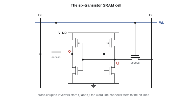
Reading begins by precharging both bit lines high. When the word line rises, the side of the cell storing 0 pulls its bit line down slowly through the access transistor and the pull-down transistor in series, and the sense amplifier detects the growing difference between the two bit lines. During the read, current flowing in from the bit line raises the 0 node slightly. If it rises past the switching threshold of the other inverter, the cell flips and the read destroys the data. To prevent this, the pull-down transistor must be stronger than the access transistor. The ratio of their strengths is the cell ratio, usually between about 1.5 and 3.
Writing works the other way. The write driver forces one bit line low, and the access transistor on that side must overpower the cell's p-channel pull-up to pull the 1 node down far enough for the loop to flip. So the access transistor must be stronger than the pull-up, a requirement described by the pull-up ratio. Reading and writing therefore place opposing demands on the access transistor, and SRAM design is a careful balance of the three transistor sizes. The figure of merit is static noise margin, the size of the largest square that fits in the eyes of the butterfly diagram from lesson 8, measured separately for holding, reading and writing.
Worked problem
Read stability of an SRAM cell
In a simplified square-law model of a 1.0 V SRAM with thresholds of 0.35 V, the access transistor is in saturation and the pull-down transistor in the linear region while a 0 is being read. With equal process transconductance, the 0 node settles where their currents match. How high does the node rise for cell ratios β of 1 and 2?
Show solution
- \[ \tfrac{1}{2}\,(V_{DD} - V - V_t)^2 = \beta\Big[(V_{DD} - V_t)\,V - \tfrac{1}{2} V^2\Big]\]
- \[ \beta = 1:\ V \approx 190\ \text{mV}, \qquad \beta = 2:\ V \approx 119\ \text{mV}\]
Answer: Doubling the pull-down strength cuts the read disturbance from about 190 mV to about 119 mV, leaving much more margin below the other inverter’s switching threshold near half the supply. Real cells must hold that margin at the worst process corner and with random variation between neighboring transistors, which is why cells are characterized statistically across millions of samples.
Variation is SRAM's central difficulty. Cell transistors are the smallest on the chip, so random differences in their thresholds are the largest, and a memory with millions of cells will contain some weak ones. Those weak cells set the minimum voltage at which the memory can operate reliably, often called V_min. That is why a microcontroller's SRAM is frequently the block that limits how far its core voltage can drop, and why retention RAM in deep sleep is held at a carefully regulated voltage.
The DRAM cell
A DRAM cell stores a bit as charge on a tiny capacitor, about 10 to 30 fF, reached through a single access transistor. One transistor and one capacitor per bit make DRAM roughly a fifth to a tenth the area of SRAM, which is why main memory is DRAM. The capacitor is built in a deep trench or as a tall stack above the transistor to get enough capacitance into a tiny footprint.
Reading a DRAM cell is a matter of charge sharing. The bit line is precharged to V_DD/2, then the word line connects the cell capacitor C_s to the much larger bit-line capacitance C_BL. The two share charge and the bit line moves a little up or down depending on whether the cell held a 1 or a 0. A sense amplifier, itself a pair of cross-coupled inverters, compares the bit line with a reference at V_DD/2, amplifies the difference to full logic levels, and in doing so writes the value back into the cell, because the read has destroyed the stored charge.
Worked problem
DRAM sense signal
A DRAM cell of 25 fF shares charge with a 100 fF bit line precharged to half of a 1.1 V supply. What signal does the sense amplifier see for a stored 1?
Show solution
- \[ \Delta V = (1.1 - 0.55)\,\text{V} \times \frac{25}{25 + 100} = 0.55 \times 0.2 = 110\ \text{mV}\]
Answer: A stored 1 raises the bit line by 110 mV and a stored 0 lowers it by the same amount. The sense amplifier must resolve that signal reliably in the presence of noise and coupling from neighboring bit lines, which is why bit lines are kept short and arranged in folded pairs that see the same noise.
The charge on the capacitor leaks away through the access transistor's subthreshold current and through junction leakage, so every cell must be read and rewritten periodically. Standard DRAM refreshes every row within 64 ms at normal temperatures, and twice as often above about 85 °C because leakage rises with temperature, as lesson 7 described. If a stored 1 may lose 0.2 V before it becomes unreadable, the worst-case leakage for a 25 fF cell is 25 fF × 0.2 V ÷ 64 ms, about 78 fA. Achieving that across billions of cells requires access transistors with very high thresholds and long channels, quite unlike logic transistors. Refresh costs power, which is why phones and laptops use low-power DRAM modes that refresh only occupied regions or slow the refresh when cool.
DRAM has its own reliability hazards. Repeatedly activating one row can disturb the cells in adjacent rows enough to flip them, an effect known as row hammer. Memory controllers and modern DRAM devices counter it by tracking frequently activated rows and refreshing their neighbors early. Error-correcting codes, which add a few check bits to each word, catch and fix the occasional flipped bit from leakage, disturbance or radiation.
Flash memory
Flash memory stores a bit as charge trapped in an insulated layer between the transistor's control gate and its channel. In the classic floating-gate cell, that layer is a conducting polysilicon gate surrounded entirely by oxide; in a charge-trap cell, it is a silicon nitride film. Electrons placed on the trapping layer shift the transistor's threshold voltage upward, and reading the cell is simply a matter of applying a gate voltage between the programmed and erased thresholds and seeing whether the transistor conducts. Because the charge is surrounded by insulator, it stays put for years with no power applied.
Moving charge through the insulator takes high fields. Programming uses either hot-carrier injection, in which electrons accelerated along the channel jump the barrier, or Fowler-Nordheim tunneling, in which a high voltage across a thin oxide lets electrons tunnel through it. Erasing removes the charge by tunneling in the reverse direction. The 10 to 20 V needed is generated on chip by charge pumps, which is one reason flash programming takes microseconds to milliseconds and draws far more current than reading. Each program and erase cycle damages the oxide slightly, trapping charge and creating leakage paths, so flash has a limited endurance, typically 10,000 to 100,000 erase cycles per block for single-bit cells, and fewer for cells that store several bits.
| Property | SRAM | DRAM | NOR flash | NAND flash |
|---|---|---|---|---|
| Cell | 6 transistors | 1 transistor, 1 capacitor | 1 transistor | 1 transistor in a series string |
| Volatile | Yes | Yes, needs refresh | No | No |
| Read access | Fastest, below 1 ns on chip | Tens of nanoseconds | Tens of nanoseconds, random access | Tens of microseconds per page |
| Write | Same as read | Same as read | Microseconds per word, erase by sector | Hundreds of microseconds per page, erase by block |
| Endurance | Unlimited | Unlimited | About 100,000 cycles | 1,000 to 100,000 cycles |
| Typical use | Caches, MCU RAM | Main memory | MCU program memory, boot code | Bulk storage, SSDs, cards |
NOR and NAND flash differ in how cells connect to the bit line. In NOR flash, each cell connects directly to its bit line, giving fast random reads, so microcontrollers execute code straight from internal NOR-type flash, with the wait states that CMP-315 configured. In NAND flash, cells are chained in series strings of 32 or more, which removes most of the contacts and greatly increases density, but reads must proceed a page at a time. NAND devices store two, three or four bits per cell by programming several distinct threshold levels, at the cost of slower writes, lower endurance and the need for strong error correction. Every NAND-based device, from a memory card to a solid-state drive, includes a controller that maps logical blocks onto physical ones, spreads erases evenly, retires bad blocks and corrects errors.
Designing with flash endurance
Flash is erased in sectors or blocks, so rewriting a single byte means erasing the whole sector and reprogramming everything in it. Firmware that ignores this can wear out a part in a surprisingly short time. Wear leveling spreads writes across many sectors, and log-structured storage appends new records instead of rewriting old ones, erasing a sector only when it fills.
Worked problem
Flash wear on the NS-5 logger
Dev Okafor's field reports show the NS-5 writes a 256-byte record every 15 minutes, 96 per day, to an external NOR flash rated for 100,000 erase cycles per 4 KB sector. Compare the lifetime if the firmware erases and rewrites one sector on every record, if it fills a sector with 16 records before erasing, and if it levels wear over 256 sectors.
Show solution
- \[ \text{rewrite every record: } \frac{100{,}000}{96\ \text{per day}} \approx 1{,}042\ \text{days} \approx 2.9\ \text{years}\]
- \[ \text{fill each sector: } \frac{100{,}000}{6\ \text{per day}} \approx 45.6\ \text{years}\]
- \[ \text{leveled over 256 sectors: } 45.6 \times 256 \approx 11{,}700\ \text{years}\]
Answer: Rewriting one sector on every record would wear out the flash in under three years, short of the node’s service life. Appending records and erasing only full sectors stretches that to decades, and spreading the erases makes endurance irrelevant. Data retention, which falls as cells wear and as temperature rises, then becomes the limiting factor.
Other non-volatile memories
Several other technologies fill niches. EEPROM, a close relative of flash with byte-level erase, stores small calibration tables and configuration. Ferroelectric RAM stores a bit in the polarization of a ferroelectric capacitor, writes at full bus speed with very low energy and survives trillions of cycles, which suits data loggers that write constantly. Magnetoresistive RAM stores a bit in the magnetic orientation of a tunnel junction and is appearing as embedded non-volatile memory in advanced microcontrollers. Each trades density, cost and process complexity against speed and endurance.
Computing memory margins with code
The code solves for the SRAM read disturbance at several cell ratios, computes the DRAM charge-sharing signal and the allowable cell leakage, and estimates flash lifetime under the three write strategies.
# Memory cells: SRAM read disturbance, DRAM charge sharing and flash wear
VDD, Vt = 1.0, 0.35

def read_bump(beta):
    # node storing 0 during a read: access device (saturated) fights pull-down (linear)
    lo, hi = 0.0, VDD - Vt
    for _ in range(60):
        v = (lo + hi) / 2
        i_acc = 0.5 * (VDD - v - Vt) ** 2
        i_pd = beta * ((VDD - Vt) * v - v * v / 2)
        lo, hi = (v, hi) if i_pd < i_acc else (lo, v)
    return v

print("SRAM read: cell ratio and voltage on the 0 node")
for beta in (1.0, 1.5, 2.0, 3.0):
    print(f"  beta = {beta:.1f}: node rises to {read_bump(beta)*1000:4.0f} mV")

# DRAM: a cell capacitor shares charge with a bit line precharged to VDD/2
Cs, Cbl, Vd = 25e-15, 100e-15, 1.1
for v_cell, name in ((Vd, "stored 1"), (0.0, "stored 0")):
    dv = (v_cell - Vd / 2) * Cs / (Cs + Cbl)
    print(f"DRAM {name}: bit line moves {dv*1000:+.0f} mV")
# leakage allowed if a stored 1 may droop 0.2 V within the 64 ms refresh interval
print(f"maximum cell leakage for 64 ms refresh: {Cs*0.2/0.064*1e15:.0f} fA")

# flash wear: 100,000 erase cycles per sector
endurance = 100_000
for label, erases_per_day in (("log rewritten in one sector every write", 96),
                              ("16 pages per sector, one sector", 6),
                              ("wear levelled over 256 sectors", 6 / 256)):
    years = endurance / erases_per_day / 365.25
print(f"{label}: {years:,.1f} years")SRAM read: cell ratio and voltage on the 0 node beta = 1.0: node rises to 190 mV beta = 1.5: node rises to 147 mV beta = 2.0: node rises to 119 mV beta = 3.0: node rises to 87 mV DRAM stored 1: bit line moves +110 mV DRAM stored 0: bit line moves -110 mV maximum cell leakage for 64 ms refresh: 78 fA log rewritten in one sector every write: 2.9 years 16 pages per sector, one sector: 45.6 years wear leveled over 256 sectors: 11,681.5 years
The numbers match the worked examples. The SRAM model shows the diminishing returns of a larger cell ratio, the DRAM results show why sense amplifiers must resolve about a tenth of a volt, and the flash results show that firmware strategy, not the chip, often determines how long stored data can be trusted.
Common mistakes
MistakeTreating SRAM sizing as a single constraint.
InsteadRead stability needs a strong pull-down; writability needs an access transistor stronger than the pull-up.
MistakeForgetting that a DRAM read is destructive.
InsteadThe sense amplifier must write the value back; refresh exists because charge leaks.
MistakeRewriting the same flash sector for every small update.
InsteadAppend records and level wear; erase cycles are finite.
MistakeIgnoring temperature when budgeting retention.
InsteadLeakage in DRAM and charge loss in flash both accelerate as temperature rises.
Summary and key terms
- Memory arrays use word lines, bit lines, decoders and sense amplifiers.
- The six-transistor SRAM cell is a bistable loop plus two access transistors.
- SRAM read stability needs a cell ratio above about 1.5; writes need an access device stronger than the pull-up.
- Random variation in tiny cell transistors sets the minimum SRAM voltage.
- A DRAM cell shares its charge with a precharged bit line; the read is destructive.
- DRAM must be refreshed, typically every 64 ms, because cell charge leaks.
- Flash traps charge in an insulated layer, shifting the threshold; erases wear the oxide.
- NOR flash gives random access for code; NAND flash gives density for storage.
- Word line
- A row line that connects every cell in a row to its bit line.
- Bit line
- A column line that carries data between cells and the sense amplifier.
- Sense amplifier
- A circuit that amplifies a small bit-line signal to a full logic level.
- Cell ratio
- The strength of an SRAM pull-down transistor relative to its access transistor.
- Static noise margin
- The largest noise voltage an SRAM cell tolerates without flipping.
- Refresh
- Periodic reading and rewriting of DRAM cells to restore leaking charge.
- Endurance
- The number of erase and program cycles a flash block survives.
- Wear leveling
- Spreading erases across many flash blocks to extend lifetime.
Practice problems
Work each problem on paper first, then reveal the answer to check.
A 20 fF DRAM cell shares charge with a 180 fF bit line at 0.6 V precharge from a 1.2 V supply. What is the signal for a stored 1?
Show answer
0.6 × 20 ÷ 200 = 60 mV.
Why must the SRAM pull-down be stronger than the access transistor?
Show answer
Otherwise current from the precharged bit line raises the 0 node past the other inverter’s threshold and flips the cell during a read.
A flash sector rated for 10,000 cycles is erased 20 times a day. How long does it last?
Show answer
500 days, about 1.4 years.
Why do NAND flash devices need a controller with error correction?
Show answer
Multi-level cells have small threshold margins and wear, so bit errors are expected and must be corrected.
Lesson quiz · 5 questions
Score 60% or more to complete this lesson.
Create a free account to save your progress, take quizzes and earn a certificate.