
CMP-350 · Lesson 5 of 12 · 19 min
CMOS logic gates and transistor sizing
The inverter generalizes into every other static CMOS gate. Replace the single n-channel transistor with a network of n-channel devices that connects the output to ground when the function should be 0, and replace the single p-channel transistor with a complementary network of p-channel devices that connects the output to the supply when the function should be 1. Arrange the two networks so that exactly one of them conducts for every input combination, and the gate draws no static current, produces full rail-to-rail outputs and regenerates its signals just as the inverter does. This lesson builds NAND, NOR and compound gates, explains why some gates are slower than others, and introduces logical effort, a method for sizing transistors and choosing the number of stages that gives the fastest path.
Pull-down and pull-up networks
In the pull-down network, n-channel transistors in series implement AND: the path to ground conducts only if all of them are on. Transistors in parallel implement OR: any one of them provides a path. The pull-up network uses p-channel transistors, which conduct when their inputs are low, and it is the dual of the pull-down network: wherever the pull-down has series devices, the pull-up has parallel ones, and the reverse. Because the output is pulled low when the pull-down conducts, a static CMOS gate always produces an inverted function. A single stage can make NAND, NOR or an AND-OR-INVERT combination; a plain AND or OR needs a second, inverting stage.
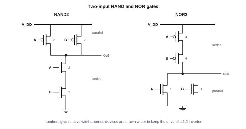
A two-input NAND gate has two n-channel transistors in series to ground and two p-channel transistors in parallel to the supply. The output falls only when both inputs are high and both series devices conduct; if either input is low, one of the parallel p-channel devices pulls the output high. A two-input NOR gate is the dual: two p-channel devices in series and two n-channel devices in parallel. Compound gates follow the same rule. An AND-OR-INVERT gate computing NOT(A·B + C) has A and B in series, in parallel with C, in the pull-down network, and the dual arrangement in the pull-up network. Compound gates often beat a cascade of simpler gates in speed and area, which is why standard-cell libraries offer dozens of them.
| Gate | Pull-down network | Pull-up network | Transistors |
|---|---|---|---|
| Inverter | 1 n-device | 1 p-device | 2 |
| NAND2 | 2 n-devices in series | 2 p-devices in parallel | 4 |
| NOR2 | 2 n-devices in parallel | 2 p-devices in series | 4 |
| NAND3 | 3 n-devices in series | 3 p-devices in parallel | 6 |
| AOI21: NOT(A·B + C) | (A series B) parallel C | (A parallel B) series C | 6 |
Sizing gates for equal drive
Transistors in series behave like resistors in series: two identical devices in series have twice the on-resistance of one. To give a NAND2 gate the same worst-case pull-down strength as a reference inverter, each of its series n-channel devices must be twice as wide. Its parallel p-channel devices only need the width of the inverter's p-channel device, because in the worst case just one of them conducts. Taking the reference inverter as an n-channel device of width 1 and a p-channel device of width 2, which balances it for a process where electrons are about twice as mobile as holes, a NAND2 then has n-channel widths of 2 and p-channel widths of 2. A NOR2 has n-channel widths of 1 and series p-channel widths of 4.
These sizes reveal why NOR gates are unpopular in CMOS. Their series p-channel transistors, already weak because of hole mobility, must be made very wide, so a NOR presents a much larger input capacitance than a NAND with the same drive. Designers therefore prefer NAND-based logic, keep series stacks short (rarely more than three or four transistors), and split wide functions into trees of smaller gates.
Logical effort
How fast a gate switches depends on how much capacitance it drives relative to how much it presents at its input, and on the gate type. Logical effort, introduced by Sutherland and Sproull, captures this in a simple delay model measured in units of τ, the delay of an ideal inverter driving an identical inverter with no parasitic capacitance. The delay of a gate is the sum of an effort delay and a parasitic delay.
Here h is the electrical effort, the ratio of the load capacitance to the gate's own input capacitance; g is the logical effort, how much worse the gate is at driving current than an inverter with the same input capacitance; and p is the parasitic delay, caused by the gate's own drain capacitance. With the sizing above, an inverter has g = 1 and p = 1. A NAND2 has input capacitance 2 + 2 = 4 against the inverter's 1 + 2 = 3, so g = 4/3. A NOR2 has 1 + 4 = 5 against 3, so g = 5/3. Larger gates have higher logical effort: a NAND3 has 5/3 and a NOR3 7/3. Parasitic delay is roughly proportional to the number of inputs, so a NAND2 or NOR2 has p of about 2.
| Gate | Logical effort g | Parasitic delay p |
|---|---|---|
| Inverter | 1 | 1 |
| NAND2 | 4/3 | 2 |
| NAND3 | 5/3 | 3 |
| NOR2 | 5/3 | 2 |
| NOR3 | 7/3 | 3 |
Optimizing a path
For a path of N gates, the logical efforts multiply into a path logical effort G, the electrical efforts multiply into the path electrical effort H, which equals the final load capacitance divided by the input capacitance of the first gate, and any fan-out to side branches contributes a branching effort B. Their product is the path effort F. The key result of the theory is that the path delay is minimized when every stage bears the same stage effort, the N-th root of F. The best stage effort turns out to be about 4, so the best number of stages is about the base-4 logarithm of F.
Once the stage effort is known, the gate sizes follow by working backward from the load. Each gate's input capacitance equals its logical effort times its output load divided by the stage effort. The result is a geometric taper: each stage a few times bigger than the one before. The same idea explains the buffer chains that drive heavy loads such as an output pad or a clock tree, where a small logic gate cannot switch a large capacitance quickly on its own.
Worked problem
Sizing a path to an output load
A NAND2, a NOR2 and an inverter drive an output load of 192 units, where one unit is the input capacitance of a minimum inverter. The NAND2 input is limited to 4 units. Find the best stage effort, the path delay and the size of each gate.
Show solution
- \[ G = \tfrac{4}{3} \times \tfrac{5}{3} \times 1 = 2.22, \qquad H = \frac{192}{4} = 48, \qquad F = 2.22 \times 48 = 106.7\]
- \[ \hat{f} = 106.7^{1/3} = 4.74, \qquad P = 2 + 2 + 1 = 5\]
- \[ D = 3 \times 4.74 + 5 = 19.2\ \tau\]
- \[ C_{\text{inv}} = \frac{1 \times 192}{4.74} = 40.5, \qquad C_{\text{nor}} = \frac{5/3 \times 40.5}{4.74} = 14.2\]
Answer: Each stage carries an effort of about 4.7, close to the ideal of 4, and the path takes about 19 τ. The gates grow from 4 to 14.2 to 40.5 units of input capacitance. A fourth stage would shave the delay only slightly and would invert the logic, so three stages is the right choice.
Fan-in, fan-out and wires
Fan-out is the number of gate inputs a single output drives; each one adds input capacitance, so a high fan-out raises the electrical effort and slows the driving gate. Fan-in is the number of inputs on one gate; it lengthens series stacks and raises both logical effort and parasitic delay. Good logic design therefore prefers trees of small gates to single wide gates, and buffers high fan-out nets such as clocks, resets and enables.
Wires add capacitance that the model must include. On a modern chip a millimeter of wire can carry as much capacitance as dozens of gate inputs, and long wires also have significant resistance, which lesson 6 analyzes. On a printed circuit board the effect is larger still: the trace from the NS-5 microcontroller to the radar module, about 8 cm long, adds roughly 8 pF plus the radar module's input capacitance of about 5 pF, compared with a few femtofarads for a gate input inside the chip. That is why output pins have large, multi-stage drivers inside the chip, and why microcontrollers let firmware choose the drive strength of each pin, which CMP-315 discussed for GPIO.
Other logic styles
Static CMOS is not the only way to build gates. Pass-transistor logic routes signals through transistors used as switches, which can build multiplexers and XOR gates with fewer transistors, at the cost of degraded levels: an n-channel pass transistor passes a strong 0 but a weak 1, reaching only V_DD − V_t. A transmission gate places an n-channel and a p-channel transistor in parallel so that both levels pass cleanly; it is the standard building block of multiplexers and the latches in lesson 8. Dynamic logic precharges the output node high on one clock phase and conditionally discharges it on the next, which is fast and compact but sensitive to noise and leakage. High-performance processors use these techniques in critical paths; microcontrollers built for low power stay mostly with static CMOS because it holds its state with no clock and tolerates slow clocks and sleep modes.
Optimizing with code
The code applies logical effort to the example path. It computes the path effort and best stage effort, sizes each gate working back from the load, and checks whether adding buffer stages would help. The same few lines can size any path once the gate types, the input limit and the load are known.
# Logical effort for a path: NAND2 -> NOR2 -> inverter driving a large load
g = {'inv': 1.0, 'nand2': 4 / 3, 'nor2': 5 / 3}
p = {'inv': 1.0, 'nand2': 2.0, 'nor2': 2.0}
path = ['nand2', 'nor2', 'inv']
C_in, C_load = 4.0, 192.0          # in units of a unit inverter's input capacitance
H = C_load / C_in
G = 1.0
for s in path:
    G *= g[s]
B = 1.0                            # no branching on this path
F = G * B * H
N = len(path)
f_hat = F ** (1 / N)
P = sum(p[s] for s in path)
D = N * f_hat + P
print(f"path logical effort G = {G:.3f}, electrical effort H = {H:.0f}")
print(f"path effort F = {F:.1f}")
print(f"best stage effort f = {f_hat:.2f}")
print(f"path delay D = {D:.1f} units (tau)")
# size each stage working backward from the load: Cin_i = g_i * Cout_i / f
c_out = C_load
sizes = []
for s in reversed(path):
    c_in = g[s] * c_out / f_hat
    sizes.append((s, c_in))
    c_out = c_in
for s, c in reversed(sizes):
    print(f"  {s:5s} input capacitance {c:6.1f}")
# would adding inverters help? compare N = 3 to 5 stages (extra inverters, p = 1 each)
for n in (3, 4, 5, 6):
    extra = n - N
    d = n * F ** (1 / n) + P + extra * 1.0
print(f"N = {n}: delay {d:.1f}")path logical effort G = 2.222, electrical effort H = 48 path effort F = 106.7 best stage effort f = 4.74 path delay D = 19.2 units (tau) nand2 input capacitance 4.0 nor2 input capacitance 14.2 inv input capacitance 40.5 N = 3: delay 19.2 N = 4: delay 18.9 N = 5: delay 19.7 N = 6: delay 21.1
The best stage effort of 4.74 is close to the ideal of 4. A four-stage path would be marginally faster at 18.9 τ, but five or more stages are slower because each added inverter brings its own parasitic delay. In practice designers accept stage efforts anywhere from about 3 to 6, because the delay curve is flat near its minimum.
Common mistakes
MistakeSizing every transistor in a gate the same width.
InsteadSeries devices need proportionally more width so the gate matches the drive of the reference inverter.
MistakeUsing wide NOR gates freely.
InsteadSeries p-channel stacks make NOR gates large and slow; prefer NAND structures and trees of small gates.
MistakeMaking the first gate of a path as big as possible.
InsteadA bigger first gate loads whatever drives it; size the path so every stage carries about the same effort.
MistakeForgetting wire capacitance in fan-out estimates.
InsteadLong on-chip wires and board traces can outweigh many gate inputs; include them in the load.
Summary and key terms
- A static CMOS gate pairs an n-channel pull-down network with a dual p-channel pull-up network.
- Series devices implement AND and parallel devices OR in the pull-down; the pull-up is the dual.
- Single-stage CMOS gates are inverting: NAND, NOR and AND-OR-INVERT.
- Series transistors must be widened to keep drive strength; NOR gates suffer most.
- Gate delay is d = gh + p in units of τ, where g is logical effort and h is electrical effort.
- A path is fastest when each stage carries equal effort, F^(1/N), ideally about 4.
- Gate sizes taper geometrically from input to load; buffer chains drive heavy loads.
- Pass transistors, transmission gates and dynamic logic trade robustness for speed or area.
- Pull-down network
- The n-channel transistors that connect a gate’s output to ground.
- Pull-up network
- The p-channel transistors that connect a gate’s output to the supply.
- Logical effort
- How much worse a gate is at driving current than an inverter of equal input capacitance.
- Electrical effort
- The ratio of a gate’s load capacitance to its input capacitance.
- Parasitic delay
- The part of a gate’s delay caused by its own internal capacitance.
- Path effort
- The product of logical, branching and electrical efforts along a path.
- Fan-out
- The number of gate inputs driven by one output.
- Transmission gate
- Parallel n- and p-channel transistors used as a switch that passes both logic levels well.
Practice problems
Work each problem on paper first, then reveal the answer to check.
What is the logical effort of a NAND4 sized for equal drive with a 1:2 reference inverter?
Show answer
n-devices width 4, p-devices width 2: input capacitance 6 versus 3, so g = 2.
An inverter with input capacitance 3 units drives 60 units. What is its delay in τ?
Show answer
h = 20, d = 1 × 20 + 1 = 21 τ.
A path has F = 256. About how many stages give the minimum delay?
Show answer
log₄ 256 = 4 stages.
Why does an n-channel pass transistor pass a weak 1?
Show answer
It turns off once its source rises to V_DD − V_t, so the output stops one threshold below the supply.
Lesson quiz · 5 questions
Score 60% or more to complete this lesson.
Create a free account to save your progress, take quizzes and earn a certificate.