
CMP-350 · Lesson 6 of 12 · 22 min
Propagation delay and RC timing
Every logic gate takes time to respond. When its input changes, the transistors that turn on must charge or discharge the capacitance hanging on the output through their own on-resistance and through the resistance of the wires. Lesson 5 treated delay in normalized units through logical effort; this lesson puts real resistances, capacitances and seconds on it. The same RC reasoning applies from the scale of a single transistor inside a chip to the scale of a reset line on a printed circuit board, and it sets the clock rate of every synchronous design.
Defining delay
Propagation delay is measured between the 50 percent points of the input and output waveforms. Because the pull-up and pull-down networks differ, a gate has two delays: t_PHL for an output falling from high to low and t_PLH for an output rising from low to high. Their average is often quoted as t_pd. Rise and fall times describe how quickly the output edge itself moves, usually between the 10 and 90 percent points, though some datasheets use 20 and 80 percent. A datasheet also distinguishes the maximum propagation delay, which the timing of a design must respect, from the minimum or contamination delay, which matters for hold-time checks in lesson 8.
| Quantity | Measured between | Used for |
|---|---|---|
| t_PHL | Input 50% to falling output 50% | Worst-case path timing |
| t_PLH | Input 50% to rising output 50% | Worst-case path timing |
| t_r, t_f | 10% and 90% of the output swing | Edge rate, signal integrity |
| t_cd (contamination) | Input change to first output change | Hold-time checks |
| t_pd | Average of t_PHL and t_PLH | Quick comparisons |
The RC step response
The simplest model of a switching gate is a resistor charging a capacitor. When a step drives a resistance R into a capacitance C, the capacitor voltage approaches its final value exponentially with time constant τ = RC. The output crosses 50 percent after ln 2 time constants, about 0.69RC, and moves from 10 to 90 percent in ln 9, about 2.2RC. These two numbers are worth memorizing, because they convert any RC estimate into a delay or an edge rate.
The transistor is not really a linear resistor. When it first turns on, it is in saturation and delivers a nearly constant current; as the output approaches the rail it enters the linear region and behaves more like a resistor. Using an effective resistance, chosen so that the RC model gives the right delay, works well in practice. A common choice is the average of the on-resistance at the start and end of the transition, and cell libraries characterize each gate at many loads and input slopes so that tools do not rely on the approximation at all.
Delay therefore depends on the supply voltage, temperature and process corner discussed in lesson 1. With the alpha-power model from lesson 3, the drive current scales as (V_DD − V_t)^α, so delay scales roughly as C V_DD / (V_DD − V_t)^α. Lowering the supply from 3.3 V to 1.8 V with a 0.5 V threshold and α = 1.3 raises the delay by a factor of about 1.48 even though the swing is smaller, which is why microcontrollers that run their core from a low-voltage regulator also limit the maximum clock frequency in each voltage range.
Elmore delay for RC networks
Real signals pass through networks of resistances and capacitances: a driver, a chain of wire segments and several gate loads. Solving such a network exactly is tedious, but Elmore showed that a good estimate of the delay to any node is the sum, over every capacitor, of the capacitance times the resistance shared between the path from the source to that capacitor and the path from the source to the node of interest. For a simple chain, that shared resistance is just the total resistance from the source up to each capacitor.
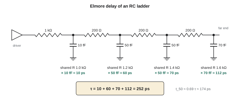
Capacitors near the source are cheap, because only a little resistance lies between them and the driver; capacitors near the far end are expensive, because they charge through everything upstream. That asymmetry has practical consequences: a large load should be placed near a strong driver, and a branch that carries a heavy load should be fed from as close to the driver as possible. Elmore delay is the first moment of the impulse response and slightly overestimates the true 50 percent delay of a distributed line, but it is easy to compute by hand and is accurate enough to rank design choices.
Worked problem
Elmore delay of a driver and wire
A driver with an effective resistance of 1 kΩ and an output capacitance of 10 fF drives a wire modeled as three segments of 200 Ω and 50 fF. A gate input of 20 fF sits at the far end. Estimate the delay to the far end.
Show solution
- \[ \tau = 1.0\,\text{k}\Omega \times 10\,\text{fF} + 1.2\,\text{k}\Omega \times 50\,\text{fF} + 1.4\,\text{k}\Omega \times 50\,\text{fF} + 1.6\,\text{k}\Omega \times 70\,\text{fF}\]
- \[ \tau = 10 + 60 + 70 + 112 = 252\ \text{ps}\]
- \[ t_{50} \approx 0.69 \times 252 = 174\ \text{ps}\]
Answer: The far-end gate switches about 174 ps after the driver input, if the single-pole conversion is used. Almost half of the Elmore sum comes from the last node, which carries both the wire and the gate load and sees the full upstream resistance.
Wires: resistance grows with length and so does capacitance
A uniform wire of length L has resistance rL and capacitance cL, where r and c are per unit length. Treated as a distributed line, its own delay is about 0.38rcL², roughly half the lumped estimate of 0.69RC, because each piece of capacitance sees only the resistance upstream of it. The square of the length is the critical point: doubling a wire's length quadruples its intrinsic delay. As processes shrink, wires get thinner and their resistance per unit length rises, so long on-chip wires have become slower relative to gates with every generation. A 10 mm wire in a modern process can take several nanoseconds unaided, while the gates that drive it switch in tens of picoseconds.
The cure is to break a long wire into segments and drive each one with a repeater, an inverter or buffer. Each segment's delay grows only with the square of its own length, so the total delay becomes linear in the length of the whole wire. The optimum spacing balances the delay of the repeaters themselves against the wire delay they eliminate; too few repeaters leave the quadratic term in place, too many add more gate delay than they save. Processors and large system chips contain thousands of repeaters, and the routing tools insert them automatically.
| Wire length | Unrepeated delay | Best segments | Repeated delay |
|---|---|---|---|
| 1 mm | 178 ps | 2 | 170 ps |
| 2 mm | 410 ps | 4 | 340 ps |
| 5 mm | 1,471 ps | 11 | 849 ps |
| 10 mm | 4,454 ps | 21 | 1,697 ps |
Board-level RC timing
On a printed circuit board, resistances are lower and capacitances higher, but the reasoning is identical. A microcontroller output pin at its high drive setting has an effective output resistance of perhaps 40 Ω. The trace from the NS-5 microcontroller to the radar module, with the radar input, totals about 13 pF, so the time constant is about 0.52 ns and the 10–90 percent rise time about 1.1 ns. At the lowest drive setting the output resistance may be ten times higher and the rise time correspondingly slower, which is often exactly what is wanted: slower edges radiate less and ring less, as lesson 12 explains.
Deliberately slow RC networks are useful too. A reset supervisor or a simple power-on reset holds a reset pin low while the supply settles, and an RC filter on a push-button input removes contact bounce before a Schmitt trigger squares the edge. For such networks the useful question is how long the capacitor takes to reach a particular threshold, not the 50 percent point.
Worked problem
An RC delay on the reset line
Ines Carvalho wants the NS-5 radar module to stay in reset until its own supply has settled. Its reset input has a threshold of 0.7 V_DD. She uses a 10 kΩ pull-up and a 100 nF capacitor. How long does the module stay in reset after the supply comes up, ignoring the supply ramp itself?
Show solution
- \[ \tau = 10\,\text{k}\Omega \times 100\,\text{nF} = 1.0\ \text{ms}\]
- \[ t = 1.0\,\text{ms} \times \ln\frac{1}{1 - 0.7} = 1.0\,\text{ms} \times 1.20 = 1.20\ \text{ms}\]
Answer: The module stays in reset for about 1.2 ms. Because the reset input threshold itself varies from part to part, typically by 10 to 20 percent, she checks the delay at the lowest and highest thresholds in the datasheet and keeps a margin above the module's required reset time. A slowly rising RC voltage can also cause a plain logic input to chatter as it passes through the threshold, which is why reset inputs normally include a Schmitt trigger.
Timing a synchronous path
Gate and wire delays add up along every path between flip-flops. In a synchronous design, the clock period must be long enough for a signal launched by one flip-flop to propagate through the slowest chain of logic and arrive at the next flip-flop before its setup time. The slowest such path is the critical path, and it sets the maximum clock frequency.
Static timing analysis tools check this inequality for every path in a design at the slow process corner, lowest voltage and highest temperature, and they check the companion hold constraint at the fast corner. Lesson 8 looks at the flip-flop side of the equation and at what happens when an asynchronous signal violates it. The practical result for a firmware or board designer is familiar: a microcontroller's maximum clock frequency is specified for each supply range and temperature range, and flash memory needs wait states once the clock period becomes shorter than its access time.
Computing delays with code
The code evaluates the Elmore delay of the example ladder and then studies a long on-chip wire. For each length it compares the unrepeated delay with the best number of repeated segments found by searching from 1 to 30. The unrepeated delay grows with the square of the length while the repeated delay grows linearly, at roughly 170 ps per millimeter for these parameters.
# Elmore delay of an RC ladder and of a long on-chip wire with repeaters
def elmore(R, C):
    # R[i], C[i]: resistance into node i and capacitance at node i (node 0 nearest the driver)
    t, r_path = 0.0, 0.0
    for r, c in zip(R, C):
        r_path += r                # resistance shared by the source and this node
        t += r_path * c
    return t

# driver 1 kOhm, three wire segments of 200 Ohm and 50 fF, gate load 20 fF at the far end
R = [1000, 200, 200, 200]
C = [10e-15, 50e-15, 50e-15, 50e-15 + 20e-15]
td = elmore(R, C)
print(f"Elmore delay to far end: {td*1e12:.0f} ps; 50% delay about {0.69*td*1e12:.0f} ps")

# long wire: r = 0.4 Ohm/um, c = 0.2 fF/um, driven by a repeater of 1 kOhm with 10 fF input
r, c = 0.4, 0.2e-15
Rd, Cd = 1000.0, 10e-15
for L_mm in (1, 2, 5, 10):
    Rw, Cw = r * L_mm * 1000, c * L_mm * 1000
    best = None
    for k in range(1, 31):
        seg = 0.69 * Rd * (Cw / k + Cd) + 0.69 * (Rw / k) * Cd + 0.38 * (Rw / k) * (Cw / k)
        t = k * seg
        if best is None or t < best[1]:
            best = (k, t)
    t1 = 0.69 * Rd * (Cw + Cd) + 0.69 * Rw * Cd + 0.38 * Rw * Cw
print(f"{L_mm:2d} mm: no repeaters {t1*1e12:6.0f} ps, best {best[0]:2d} segments {best[1]*1e12:5.0f} ps")Elmore delay to far end: 252 ps; 50% delay about 174 ps 1 mm: no repeaters 178 ps, best 2 segments 170 ps 2 mm: no repeaters 410 ps, best 4 segments 340 ps 5 mm: no repeaters 1471 ps, best 11 segments 849 ps 10 mm: no repeaters 4454 ps, best 21 segments 1697 ps
The results confirm the hand calculation of 252 ps for the ladder and show the crossover at which repeaters pay off. At 1 mm, repeaters barely help; at 10 mm, they cut the delay by more than a factor of 2.5. On a board the same trade-off appears as the choice between one strong driver and a buffer placed partway along a long, heavily loaded net, such as a clock that fans out to many devices.
Common mistakes
MistakeUsing 0.69RC for a distributed wire.
InsteadA uniform distributed line has an intrinsic delay of about 0.38RC; the lumped figure overestimates it.
MistakePlacing a heavy load at the far end of a long, resistive branch.
InsteadCapacitance far from the driver is weighted by all the upstream resistance; feed heavy loads from near the driver.
MistakeAssuming delay falls in proportion to the voltage swing when the supply is lowered.
InsteadDrive current falls faster than the swing, so lower supplies make gates slower.
MistakeTiming an RC reset delay to the 50 percent point.
InsteadUse the actual input threshold and its tolerance, and remember a Schmitt trigger is needed on slow edges.
Summary and key terms
- Propagation delay is measured between 50 percent points; rise and fall times between 10 and 90 percent.
- An RC step response crosses 50 percent at 0.69RC and rises from 10 to 90 percent in 2.2RC.
- Delay scales roughly as C V_DD / (V_DD − V_t)^α, so lower supplies and slow corners are slower.
- Elmore delay sums each capacitance times the resistance it shares with the path to the node.
- An unrepeated wire’s delay grows with the square of its length; repeaters make it linear.
- Board nets follow the same RC rules with larger capacitances and lower resistances.
- Threshold-based RC delays use t = RC ln(V_DD / (V_DD − V_th)).
- The clock period must cover clock-to-Q delay, the slowest logic path and setup time.
- Propagation delay
- The time from an input crossing 50 percent to the output crossing 50 percent.
- Rise time
- The time for an edge to move between 10 and 90 percent of its swing.
- Contamination delay
- The shortest time from an input change to any output change.
- Elmore delay
- An estimate of RC network delay from each capacitance and its shared upstream resistance.
- Distributed RC line
- A wire whose resistance and capacitance are spread along its length.
- Repeater
- A buffer inserted along a long wire to make its delay grow linearly with length.
- Critical path
- The slowest register-to-register path, which sets the maximum clock frequency.
- Static timing analysis
- Checking every path’s setup and hold constraints without simulation.
Practice problems
Work each problem on paper first, then reveal the answer to check.
A 2 kΩ effective resistance drives 50 fF. What are the 50 percent delay and the 10–90 percent rise time?
Show answer
RC = 100 ps, so t₅₀ ≈ 69 ps and t_r ≈ 220 ps.
A wire's intrinsic delay is 40 ps at 1 mm. What is it at 3 mm without repeaters?
Show answer
Delay grows with the square of length: 9 × 40 = 360 ps.
A 100 kΩ pull-up and 1 µF capacitor feed an input with a 0.5 V_DD threshold. How long until it switches?
Show answer
τ = 100 ms; t = 100 ms × ln 2 ≈ 69 ms.
Clock-to-Q is 0.3 ns, setup 0.2 ns and the slowest logic 4.5 ns. What is the maximum clock frequency?
Show answer
T = 5.0 ns, so 200 MHz.
Lesson quiz · 5 questions
Score 60% or more to complete this lesson.
Create a free account to save your progress, take quizzes and earn a certificate.