
CMP-350 · Lesson 8 of 12 · 23 min
Latches, flip-flops and metastability at the circuit level
Combinational gates compute; storage elements remember. Every register, state machine and pipeline stage in a processor depends on latches and flip-flops, and their timing parameters, setup time, hold time and clock-to-output delay, appear in every timing calculation. CMP-240 treated flip-flops as logic symbols with ideal behavior. This lesson opens them up to show how two cross-coupled inverters store a bit, how transmission gates build latches and flip-flops, where setup and hold times come from, and why a flip-flop sampling an asynchronous signal can hang between 0 and 1 for an unpredictable time.
Bistability: two inverters in a loop
Connect the output of one inverter to the input of a second and the output of the second back to the first. The loop has two stable states, one with the first output high and the second low, and the reverse. Each inverter's high gain near the switching threshold, which lesson 4 measured at more than 30, pushes any small disturbance back toward one of the rails. The loop also has a third equilibrium where both nodes sit at the switching threshold V_M. That point is unstable: like a ball balanced on a hilltop, the slightest push sends it rolling to one side. This unstable point is the root of metastability.
Plotting the transfer curve of one inverter together with the mirrored transfer curve of the other gives the butterfly diagram used to analyze SRAM cells in lesson 9. The two curves cross at three points: the two stable states near the corners and the metastable point in the middle. The size of the eyes between the curves measures how much noise the loop can tolerate before it flips.
Latches
A storage loop is useful only if it can be written. The SR latch built from two cross-coupled NOR gates sets when S is high and resets when R is high; asserting both at once is forbidden because releasing them together leaves the latch in a race. A gated D latch removes the forbidden state. In CMOS it is usually built with transmission gates: when the clock is high, one transmission gate passes the D input to the storage node and the latch is transparent, with Q following D; when the clock falls, that gate opens and a second transmission gate closes the feedback loop, so the value present at the moment of the clock edge is held.
| Element | Captures data | Typical CMOS transistor count | Main use |
|---|---|---|---|
| SR latch (NOR) | Whenever S or R is asserted | 8 | Debouncing, simple set-reset flags |
| D latch | While the clock is high (transparent) | 8 to 12 | Latch-based pipelines, clock gating cells |
| Master-slave D flip-flop | At the clock edge | 16 to 24 | Registers in synchronous logic |
| Flip-flop with reset and enable | At the clock edge, if enabled | 24 to 30 | Control registers, state machines |
The master-slave flip-flop
An edge-triggered D flip-flop chains two latches with opposite clock phases. The master latch is transparent while the clock is low and follows D; the slave latch is opaque and holds the previous output. When the clock rises, the master closes and holds the value of D at that instant, while the slave opens and passes the held value to Q. The output therefore changes only just after the rising edge. Because the two latches are never transparent at the same time, data cannot race straight through, provided the clock edges are clean and the two clock phases do not overlap significantly.
The timing parameters follow directly from this structure. The setup time is how long D must be stable before the clock edge so that the master's storage node has charged fully to the new value before its input gate closes. The hold time is how long D must stay stable after the edge, because the input transmission gate takes a little time to turn off and a change arriving in that window could still leak through. The clock-to-Q delay is the time for the slave to pass the stored value through its transmission gate and output inverter. All three depend on voltage, temperature and process corner like any other delay.
The second inequality is the hold constraint. It does not involve the clock period at all, so a hold violation cannot be fixed by slowing the clock: if data from one flip-flop can race through a very short path and arrive at the next before that flip-flop has finished capturing the previous value, the circuit fails at every frequency. Clock skew, the difference in arrival time of the clock at the two flip-flops, worsens hold problems when the capturing flip-flop's clock arrives late. Tools fix hold violations by inserting delay buffers in the short paths.
Worked problem
Setup and hold slack
A path between two flip-flops on a 100 MHz clock has a slowest logic delay of 7.6 ns and a fastest logic delay of 0.15 ns. The flip-flops have t_clk→Q of 0.5 ns (minimum 0.35 ns), setup 0.3 ns and hold 0.25 ns. The clock arrives at the capturing flip-flop 0.4 ns after the launching one. Check both constraints, treating the skew as hurting each check.
Show solution
- \[ \text{setup: } 0.5 + 7.6 + 0.3 + 0.4 = 8.8\ \text{ns} \le 10\ \text{ns}, \qquad \text{slack} = 1.2\ \text{ns}\]
- \[ \text{hold: } 0.35 + 0.15 = 0.50\ \text{ns} \quad\text{versus}\quad 0.25 + 0.4 = 0.65\ \text{ns}\]
- \[ \text{hold slack} = 0.50 - 0.65 = -0.15\ \text{ns}\]
Answer: Setup passes with 1.2 ns to spare, but hold fails by 0.15 ns. Running the clock slower would not help; the fix is to add at least 0.15 ns of delay to the short path, or to reduce the skew. Strictly, late capture clock skew helps setup rather than hurting it, so this treatment of setup is conservative.
Metastability
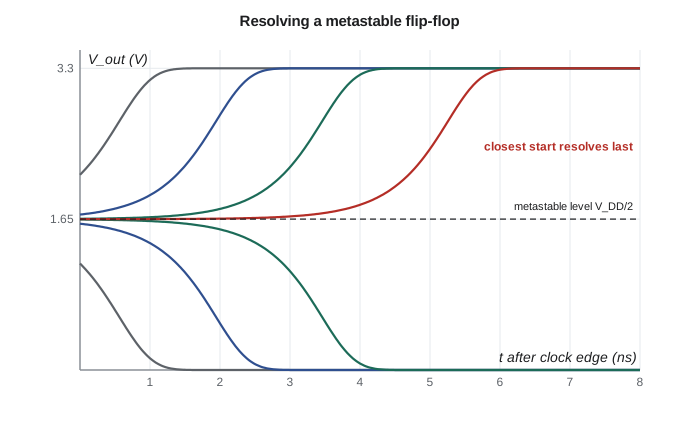
Setup and hold times are promises the designer makes to the flip-flop. When data comes from a different clock domain, or from the outside world, such as a push button, a radar module's interrupt line or a UART receive pin, no such promise is possible. Sooner or later an input edge will arrive inside the tiny window around the clock edge, and the master latch will close with its storage node partway between 0 and 1, near the unstable equilibrium. The loop then sits there while its gain slowly amplifies the small difference between the two nodes, and the output can remain at an invalid level, oscillate, or resolve to either value after a delay much longer than the normal clock-to-Q.
Near the metastable point, the cross-coupled pair behaves like a linear amplifier with positive feedback. A small voltage difference grows exponentially with a time constant τ set by the node capacitance divided by the transconductance of the inverters, typically tens to a couple of hundred picoseconds depending on the process. The probability that the flip-flop has still not resolved after a time t therefore falls as e^(−t/τ). That exponential is both the bad news and the good news: no finite wait guarantees resolution, but each additional multiple of τ cuts the probability of failure by a factor of e.
Mean time between failures
The standard model gives the mean time between synchronizer failures in terms of the resolution time allowed, the time constant τ, an aperture T_w that measures how wide the dangerous window is, the clock frequency and the rate of asynchronous data edges.
Worked problem
Synchronizing the radar interrupt line
Jonah Abara is reviewing how the NS-5 samples the radar module's data-ready line, which toggles asynchronously about 10,000 times a second. The microcontroller clock is 48 MHz. For its flip-flops take τ = 150 ps and T_w = 100 ps, t_clk→Q = 0.5 ns and setup 0.3 ns. Compare a single flip-flop feeding logic that leaves only 2 ns of slack with a two-flip-flop synchronizer.
Show solution
- \[ \text{one flop: } \text{MTBF} = \frac{e^{2/0.15}}{100\,\text{ps} \times 48\,\text{MHz} \times 10\,\text{kHz}} = \frac{6.2 \times 10^{5}}{48} \approx 1.3 \times 10^{4}\ \text{s}\]
- \[ t_r = 20.83 - 0.5 - 0.3 = 20.03\ \text{ns}\]
- \[ \text{two flops: } \text{MTBF} = \frac{e^{20.03/0.15}}{48} \approx 6.6 \times 10^{48}\ \text{years}\]
Answer: A single flip-flop would fail about every 3.6 hours, which in the field looks like a rare, unreproducible glitch. The second flip-flop gives the first a whole clock period to resolve and pushes the failure rate far beyond any meaningful lifetime. This is why microcontroller GPIO inputs pass through a two-stage synchronizer, adding a cycle or two of latency that CMP-315 noted when measuring interrupt response.
The exponential makes the result sensitive to the clock period. Running the same flip-flops at 200 MHz leaves only 4.2 ns to resolve and the MTBF falls to a couple of centuries; at 300 MHz it falls to under a day. Fast processes have much smaller τ, so real high-speed designs are not that bad, but the lesson holds: at high clock rates or in safety-critical systems, designers use three-stage synchronizers or flip-flops specially characterized for synchronization.
Crossing clock domains safely
A two-flip-flop synchronizer is correct for a single, slowly changing control bit. It is wrong for a multi-bit bus, because each bit may resolve differently and the receiving domain can see a mixture of old and new values. Safe multi-bit crossings use one of a few patterns. A handshake sends a single request bit through a synchronizer, the receiver captures the stable data bus and returns an acknowledge through another synchronizer. An asynchronous FIFO passes its read and write pointers between domains in Gray code, in which consecutive values differ in only one bit, so a pointer caught mid-change is either the old or the new value, never a wild one. A pulse in a fast domain may be too short for a slow domain to see, so it is first stretched into a level or converted into a toggle.
Resets need care as well. A reset that is asserted asynchronously works immediately, even with no clock, but releasing it asynchronously can put flip-flops in different states if the release lands near a clock edge. The standard practice is asynchronous assertion with synchronous deassertion: the reset signal passes through a small synchronizer so that its release is aligned with the clock, and every flip-flop leaves reset in the same cycle.
| Crossing | Safe method | Unsafe shortcut |
|---|---|---|
| Single slow control bit | Two- or three-flip-flop synchronizer | Direct connection to logic |
| Multi-bit data bus | Handshake or asynchronous FIFO | Synchronizing each bit separately |
| Counter or pointer | Gray code, then synchronize | Binary count through synchronizers |
| Short pulse into slower domain | Pulse stretcher or toggle synchronizer | Hoping the slow clock samples it |
| Reset release | Asynchronous assert, synchronous deassert | Fully asynchronous release |
Computing MTBF with code
The code evaluates the MTBF formula for the three synchronizer depths and then for a two-stage synchronizer as the clock frequency rises. Because the result spans more than a hundred orders of magnitude, it prints short times in seconds and long ones in years.
# Metastability: mean time between synchronizer failures
import math

def mtbf(t_res, tau, t_w, f_clk, f_data):
    return math.exp(t_res / tau) / (t_w * f_clk * f_data)

tau, t_w = 150e-12, 100e-12      # resolution time constant and aperture of the flip-flop
f_clk, f_data = 48e6, 10e3       # sampling clock and rate of asynchronous input edges
T = 1 / f_clk
t_cq, t_su = 0.5e-9, 0.3e-9
year = 365.25 * 24 * 3600

cases = [("one flop, 2 ns of slack to logic", 2e-9),
         ("two flops, one full cycle to resolve", T - t_cq - t_su),
         ("three flops, two cycles to resolve", 2 * (T - t_cq - t_su))]
for name, t_res in cases:
    m = mtbf(t_res, tau, t_w, f_clk, f_data)
    if m < year:
        print(f"{name}: MTBF {m:.3g} s ({m/3600:.1f} hours)")
    else:
        print(f"{name}: MTBF {m/year:.3g} years")

# how the two-flop result degrades at a faster clock
for f in (48e6, 100e6, 200e6, 300e6):
    t_res = 1 / f - t_cq - t_su
    m = mtbf(t_res, tau, t_w, f, f_data)
print(f"{f/1e6:6.0f} MHz clock: resolution {t_res*1e9:5.2f} ns, MTBF {m/year:.3g} years")one flop, 2 ns of slack to logic: MTBF 1.29e+04 s (3.6 hours)
two flops, one full cycle to resolve: MTBF 6.64e+48 years
three flops, two cycles to resolve: MTBF 6.68e+106 years
48 MHz clock: resolution 20.03 ns, MTBF 6.64e+48 years
100 MHz clock: resolution 9.20 ns, MTBF 1.37e+17 years
200 MHz clock: resolution 4.20 ns, MTBF 229 years
300 MHz clock: resolution 2.53 ns, MTBF 0.00228 yearsThe table of results makes the exponential concrete. Moving from one stage to two improves reliability by more than fifty orders of magnitude at 48 MHz, while raising the clock from 100 to 300 MHz with the same flip-flops undoes almost all of that improvement. The model's parameters τ and T_w come from characterization of the specific flip-flop; the values here are illustrative.
Common mistakes
MistakeFixing a hold violation by lowering the clock frequency.
InsteadHold does not depend on the clock period; add delay to the short path or reduce skew.
MistakeSynchronizing each bit of a multi-bit bus separately.
InsteadThe bits can resolve in different cycles; use a handshake, Gray code or an asynchronous FIFO.
MistakeAssuming a flip-flop always resolves within its clock-to-Q delay.
InsteadA metastable flip-flop can take an unbounded time; only the probability falls exponentially.
MistakeReleasing reset asynchronously.
InsteadFlip-flops may leave reset in different cycles; synchronize the deassertion.
Summary and key terms
- Two cross-coupled inverters form a bistable loop with an unstable midpoint.
- A D latch is transparent while its clock is active; transmission gates switch it between pass and hold.
- A master-slave flip-flop chains two latches on opposite clock phases to capture at an edge.
- Setup and hold times arise from the time the master needs to settle and its input gate needs to close.
- Hold violations do not depend on clock period; setup violations do.
- Metastability resolves exponentially with a time constant τ set by node capacitance and gain.
- MTBF = e^(t_r/τ) / (T_w f_clk f_data); each extra synchronizer stage adds a full clock period.
- Multi-bit crossings need handshakes, Gray-coded pointers or asynchronous FIFOs.
- Bistable
- Having two stable states, like a pair of cross-coupled inverters.
- Transparent latch
- A latch whose output follows its input while the clock is active.
- Setup time
- How long data must be stable before the clock edge.
- Hold time
- How long data must remain stable after the clock edge.
- Clock skew
- The difference in clock arrival time between two flip-flops.
- Metastability
- A flip-flop state near the unstable midpoint that takes an unpredictable time to resolve.
- Synchronizer
- A chain of flip-flops that gives a metastable sample time to resolve.
- Gray code
- A binary ordering in which consecutive values differ in only one bit.
Practice problems
Work each problem on paper first, then reveal the answer to check.
A path has t_clk→Q 0.4 ns, logic 3.1 ns, setup 0.2 ns and skew 0.1 ns. What is the shortest clock period?
Show answer
3.8 ns, about 263 MHz.
If τ = 100 ps, how much does each additional nanosecond of resolution time improve MTBF?
Show answer
By e¹⁰ ≈ 22,000 times.
Why is Gray code used for FIFO pointers crossing clock domains?
Show answer
Only one bit changes per increment, so a pointer caught mid-change reads as the old or the new value.
A hold check fails by 80 ps. Does halving the clock frequency fix it?
Show answer
No; hold is independent of the clock period. Add delay or reduce skew.
Lesson quiz · 5 questions
Score 60% or more to complete this lesson.
Create a free account to save your progress, take quizzes and earn a certificate.