
CMP-350 · Lesson 11 of 12 · 27 min
Interfacing to the analog world: drivers, switches and isolation
A microcontroller pin can source or sink a few milliamps at its supply voltage. The things a computer engineer wants to control rarely fit inside that limit: a valve coil at 12 V and half an amp, a modem that pulls 0.45 A in bursts, a motor, a heater, a relay, or a sensor that must be electrically isolated from the rest of the system. This lesson covers the circuits that sit between logic and those loads: transistor switches and their gate drive, protection against inductive kickback, load switches that tame inrush current, analog switches for routing signals, and isolators that carry data across a voltage barrier. ELE-240 Electronics I treats the bipolar transistor as a switch and amplifier in depth; here the focus is on the MOSFET circuits most common in digital products.
What a GPIO pin can drive
A typical microcontroller output can drive 4 to 20 mA per pin while keeping its output within the guaranteed levels, with a lower limit on the total current through all pins of a port and through the chip's supply pins. Beyond those limits, the output voltage sags away from the rail, the chip heats and the supply bond wires carry more current than they were designed for. The output resistance at each drive setting, about 25 to 100 Ω at high drive, is what limits the current into a short circuit. Small LEDs, logic inputs and the gates of MOSFETs are within reach; almost anything that does real work is not, and needs a switch.
The low-side MOSFET switch
The simplest power switch is an n-channel enhancement MOSFET with its source to ground and its drain to the low side of the load, the load's other end going to the supply. A logic-high gate turns the transistor on and current flows; a logic-low gate turns it off. Because the source sits at ground, the gate-to-source voltage equals the logic level, so a 3.3 V output can drive the switch directly, provided the MOSFET is specified as a logic-level device with its on-resistance guaranteed at a gate-to-source voltage of 2.5 or 3.3 V. A part specified only at 10 V may be barely on at 3.3 V and may overheat.
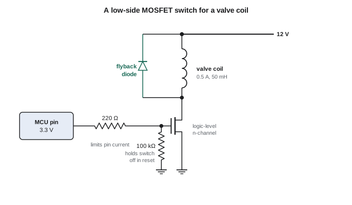
Two small parts complete the circuit. A pull-down resistor of 10 to 100 kΩ from gate to ground keeps the switch off while the microcontroller is in reset and its pins float, the state CMP-315 described at power-up. A series gate resistor of tens to hundreds of ohms limits the current spike from the pin into the gate capacitance and damps ringing between that capacitance and the trace inductance. The MOSFET's on-resistance sets the conduction loss, I²R_on, which for small loads is tiny, and its gate charge sets how quickly it switches.
Worked problem
A valve driver for the NS-5
The NS-5 variant for water monitoring opens a 12 V sampling valve whose coil draws 0.5 A. Ines Carvalho picks a logic-level MOSFET with R_on = 60 mΩ at 3.3 V gate drive, a Miller charge Q_gd of 2 nC and a Miller plateau near 1.8 V. The pin has about 40 Ω of output resistance and she adds a 220 Ω gate resistor. Find the conduction loss and the time the drain takes to switch.
Show solution
- \[ P = I^2 R_{\text{on}} = (0.5\,\text{A})^2 \times 60\,\text{m}\Omega = 15\ \text{mW}\]
- \[ I_G = \frac{3.3 - 1.8}{220 + 40} = 5.77\ \text{mA}\]
- \[ t_{\text{sw}} \approx \frac{Q_{gd}}{I_G} = \frac{2\,\text{nC}}{5.77\,\text{mA}} \approx 347\ \text{ns}\]
Answer: The conduction loss is only 15 mW, so no heat sink is needed. While the drain voltage swings, the gate sits on its Miller plateau and the gate current must charge the gate-to-drain capacitance; that sets a transition of about 0.35 µs. For a valve switched a few times a day the switching loss is irrelevant, and the slow edge even helps with emissions.
Switching loss matters when the switch is pulse-width modulated, as for dimming a lamp or controlling a heater or fan. During each transition the transistor carries current and voltage at once, dissipating roughly ½VIt_sw per edge. With the values above, PWM at 1 kHz adds 2 mW, at 20 kHz about 42 mW and at 100 kHz about 208 mW, overtaking the conduction loss many times over. Fast PWM therefore needs a gate driver chip that can source and sink amperes into the gate, rather than a GPIO pin through a resistor.
Inductive loads and flyback
Coils store energy in their magnetic field, ½LI². When a switch interrupts the current, the inductor keeps that current flowing for an instant and its voltage rises as far as necessary to do so, easily reaching hundreds of volts and destroying the switch through avalanche breakdown. A flyback diode across the coil, cathode to the supply, gives the current a path: at turn-off the coil's lower end rises one diode drop above the supply and the current circulates through the diode and the coil's own resistance until the energy is spent.
The simple diode clamp is gentle but slow. The current decays with the coil's own time constant L/R, which for a 50 mH coil of 24 Ω is about 2.1 ms, so the current takes about 6 ms to fall to a few percent. During that time a relay's contacts or a valve's plunger stay held, slowing the release. Adding a Zener diode in series with the flyback diode raises the clamp voltage, so the current falls much faster, in roughly LI/V_clamp, at the cost of a higher voltage on the switch. With a 24 V Zener the current collapses in about 1 ms, and the MOSFET must then withstand the supply plus the clamp, about 36.7 V, so a 60 V part is the natural choice.
| Clamp | Switch voltage at turn-off | Current decay | Use |
|---|---|---|---|
| None | Hundreds of volts, avalanche | Uncontrolled | Never acceptable |
| Diode | Supply + 0.7 V | Slow, about 3L/R | Relays and valves where release time does not matter |
| Diode + Zener | Supply + V_Z + 0.7 V | Fast, about LI/V_clamp | Faster release; switch rated for the higher voltage |
| Avalanche-rated MOSFET | Breakdown voltage | Fast | Clamping energy absorbed in the switch; check its rating |
High-side load switches and inrush
Some loads must be switched on their supply side: a sensor or modem whose ground must stay connected to the rest of the circuit, or a whole subsystem that should be unpowered while the node sleeps. A high-side switch uses a p-channel MOSFET with its source on the supply; pulling its gate low turns it on. When the supply is higher than the logic voltage, a small n-channel transistor or a dedicated level shifter pulls the p-channel gate down, because a 3.3 V pin cannot turn off a p-channel transistor whose source sits at 12 V. Integrated load switches package the MOSFET, its gate drive, protection and a controlled turn-on into one small chip.
Controlled turn-on matters because the load usually has bulk capacitance. Connecting a 100 µF capacitor to a 3.8 V rail through a switch with 0.1 Ω of resistance would start a current of 38 A, collapsing the source rail and possibly resetting the microcontroller that issued the command. Load switches therefore ramp their output voltage slowly. The inrush current is the capacitance times the rate of rise, so a chosen ramp time sets it.
Worked problem
Soft-starting the modem rail
The NS-5 modem sits behind a load switch so that it is fully unpowered between its eight bursts per hour. Its rail is 3.8 V with 100 µF of bulk capacitance to supply the 0.45 A transmit peaks. Dana Okoye wants the turn-on inrush held to 0.2 A, below the modem's own peak. What ramp time is needed?
Show solution
- \[ t_{\text{ramp}} = \frac{100\,\mu\text{F} \times 3.8\,\text{V}}{0.2\,\text{A}} = 1.9\ \text{ms}\]
Answer: A 1.9 ms ramp keeps the inrush to 0.2 A. Many integrated load switches set the ramp with a small external capacitor or offer fixed slew rates; one with a ramp of about 2 ms, or longer, is suitable. The ramp adds a couple of milliseconds to each modem wake-up, negligible against the 40 ms burst, and the firmware must wait for the rail’s power-good signal before talking to the modem.
Analog switches and multiplexers
CMOS transmission gates, met in lesson 5, also route analog signals. An analog switch is a transmission gate with its n-channel and p-channel transistors sized so that the combined on-resistance is reasonably flat across the signal range. Analog multiplexers select one of several sensors into a single ADC, and microcontrollers contain them in front of their ADCs. Three properties matter. On-resistance, from a few ohms to a few hundred, forms an RC filter with the following capacitance and drops voltage with current. Charge injection is the small packet of charge pushed onto the signal as the switch's gates change state, which produces a step error on a small hold capacitor. Leakage current through an off switch adds error when source impedances are high.
The microcontroller ADC's own input is a switched capacitor: at the start of each sample it connects a small sampling capacitor, a few picofarads, to the pin, drawing a burst of charge. A high-impedance sensor cannot recharge that capacitor within the sampling time, so the reading is low. CMP-315 covered the remedy from the firmware side, longer sampling times; from the hardware side, a capacitor of 10 to 100 times the sampling capacitance directly at the pin acts as a charge reservoir, or an op-amp buffer presents a low source impedance.
Isolation
Sometimes the two sides of an interface must not share a ground: a sensor at a distant point with a different ground potential, a line-powered circuit, a medical electrode, or a noisy motor drive. Galvanic isolation carries information across a barrier with no conducting path. The optocoupler sends it as light: an LED on the input side shines on a phototransistor on the output side. Its key specification is the current transfer ratio, the output collector current divided by the LED current, which varies widely from part to part, falls with temperature and declines as the LED ages.
Worked problem
Sizing an optocoupler output
Dev Okafor connects a remote alarm contact to the NS-5 through an optocoupler. The LED is driven at 5 mA and the minimum current transfer ratio over temperature and life is 50 percent. The phototransistor pulls a 3.3 V input low through a pull-up resistor and must reach 0.4 V. What is the smallest pull-up that guarantees a valid low?
Show solution
- \[ I_C = 0.5 \times 5\,\text{mA} = 2.5\ \text{mA}\]
- \[ R \ge \frac{3.3 - 0.4}{2.5\,\text{mA}} = 1{,}160\ \Omega\]
Answer: Any pull-up of 1,160 Ω or more guarantees the phototransistor can pull the line low. A 2.2 kΩ resistor gives margin while keeping the rising edge reasonably fast, a time constant of about 110 ns with 50 pF of capacitance; a 10 kΩ resistor would save current but slow the edge to about 500 ns. Optocouplers are slow, typically switching in microseconds, so they suit alarm contacts and slow serial links but not fast buses.
For faster data, digital isolators carry signals across a thin glass or polymer barrier using capacitive or magnetic coupling, at tens to hundreds of megabits per second and with much better aging and timing than optocouplers. Isolated DC-DC converters carry power across the same kind of barrier, so an isolated sensor interface can be built entirely from small chips. Isolation components are specified by the voltage they withstand across the barrier and by creepage and clearance, the surface and air distances between the two sides on the board, which the layout must preserve.
| Device | Speed | Strengths | Weaknesses |
|---|---|---|---|
| Optocoupler | Kilohertz to a few megahertz | Simple, cheap, high isolation voltage | Transfer ratio varies and degrades; slow |
| Capacitive digital isolator | Up to about 150 Mbit/s | Fast, low power, stable over life | Needs a supply on each side |
| Magnetic digital isolator | Up to about 150 Mbit/s | Fast, can integrate power transfer | Needs a supply on each side |
| Relay | Milliseconds | Switches large loads, very low on-resistance | Contacts wear; coil needs a driver |
Computing driver values with code
The code reproduces the lesson's driver calculations: conduction and switching losses for the low-side switch, energy and decay times for the coil with two clamps, the inrush ramp for the modem rail and the optocoupler pull-up.
# Driving loads from logic: MOSFET switch, flyback, inrush and optocoupler sizing
import math

# low-side switch for a 12 V valve coil drawing 0.5 A, MOSFET R_on 60 mOhm at V_GS = 3.3 V
I, R_on, V = 0.5, 0.060, 12.0
print(f"conduction loss {I*I*R_on*1e3:.0f} mW, drop {I*R_on*1e3:.0f} mV")
Q_gd, R_gate, V_gpio, R_pin, V_plat = 2e-9, 220.0, 3.3, 40.0, 1.8   # Miller charge, gate resistor, pin resistance, plateau
print(f"peak gate current {V_gpio/(R_gate+R_pin)*1e3:.1f} mA")
I_gate = (V_gpio - V_plat) / (R_gate + R_pin)      # current during the Miller plateau
t_sw = Q_gd / I_gate
print(f"plateau gate current {I_gate*1e3:.2f} mA, drain transition about {t_sw*1e9:.0f} ns")
for f in (1e3, 20e3, 100e3):
    p_sw = 0.5 * V * I * 2 * t_sw * f                   # rising plus falling transition
    print(f"PWM at {f/1e3:5.0f} kHz: switching loss {p_sw*1e3:.2f} mW")

# flyback: coil inductance 50 mH; diode clamp versus diode plus 24 V zener
L = 50e-3
R_coil = V / I
print(f"coil energy {0.5*L*I*I*1e3:.2f} mJ, decay with diode about {3*L/R_coil*1e3:.1f} ms (3 L/R)")
V_z = 24.0
print(f"with a {V_z:.0f} V zener the current falls in about {L*I/(V_z+0.7)*1e3:.2f} ms; switch sees {V+V_z+0.7:.1f} V")

# inrush: load switch charging 100 uF on a 3.8 V modem rail
C, V_rail = 100e-6, 3.8
print(f"hard switch-on through 0.1 ohm: peak {V_rail/0.1:.0f} A")
for I_lim in (0.2, 0.5):
    print(f"ramp for {I_lim} A inrush: {C*V_rail/I_lim*1e3:.2f} ms")

# optocoupler: LED at 5 mA, minimum current transfer ratio 50 %
I_led, ctr, V_out, V_ce_sat = 5e-3, 0.5, 3.3, 0.4
I_c = I_led * ctr
R_min = (V_out - V_ce_sat) / I_c
print(f"collector current {I_c*1e3:.1f} mA, pull-up at least {R_min:.0f} ohm")
for R in (2200, 10000):
print(f" pull-up {R} ohm: rise time constant with 50 pF about {R*50e-12*1e9:.0f} ns")conduction loss 15 mW, drop 30 mV peak gate current 12.7 mA plateau gate current 5.77 mA, drain transition about 347 ns PWM at 1 kHz: switching loss 2.08 mW PWM at 20 kHz: switching loss 41.60 mW PWM at 100 kHz: switching loss 208.00 mW coil energy 6.25 mJ, decay with diode about 6.3 ms (3 L/R) with a 24 V zener the current falls in about 1.01 ms; switch sees 36.7 V hard switch-on through 0.1 ohm: peak 38 A ramp for 0.2 A inrush: 1.90 ms ramp for 0.5 A inrush: 0.76 ms collector current 2.5 mA, pull-up at least 1160 ohm pull-up 2200 ohm: rise time constant with 50 pF about 110 ns pull-up 10000 ohm: rise time constant with 50 pF about 500 ns
The results show how the dominant concern changes with the application. For a valve switched occasionally, conduction loss is everything; for PWM, switching loss quickly dominates; for an inductive load, the clamp sets both the switch's voltage rating and how fast the load releases; and for a capacitive load, the inrush current set by the ramp decides whether the supply survives switch-on.
Common mistakes
MistakeDriving a standard MOSFET from a 3.3 V pin.
InsteadUse a logic-level part with R_on specified at the available gate voltage.
MistakeLeaving a MOSFET gate floating during reset.
InsteadAdd a gate pull-down so the load stays off while pins are high impedance.
MistakeSwitching an inductive load without a clamp.
InsteadThe kickback voltage will avalanche the switch; add a flyback diode, with a Zener for faster release.
MistakeHard-switching a load with large bulk capacitance.
InsteadUse a load switch with a controlled ramp to limit inrush current.
MistakeSizing an optocoupler pull-up from the typical transfer ratio.
InsteadUse the minimum over temperature and life.
Summary and key terms
- GPIO pins drive only milliamps; real loads need transistor switches.
- A low-side n-channel MOSFET needs a logic-level rating, a gate pull-down and a small gate resistor.
- Conduction loss is I²R_on; PWM adds switching loss proportional to frequency.
- Inductive loads need a flyback clamp; a Zener speeds release but raises switch voltage.
- High-side switches and load switches power whole subsystems on and off.
- Inrush current equals C dV/dt; controlled ramps protect the supply.
- Analog switches have on-resistance, charge injection and leakage; ADC inputs draw charge bursts.
- Optocouplers and digital isolators carry data across an isolation barrier.
- Logic-level MOSFET
- A MOSFET whose on-resistance is specified at logic gate voltages such as 2.5 or 3.3 V.
- Low-side switch
- A switch between a load and ground.
- High-side switch
- A switch between the supply and a load.
- Miller plateau
- The gate voltage that holds steady while the drain swings during switching.
- Flyback diode
- A diode across an inductive load that carries its current at switch-off.
- Inrush current
- The surge drawn when a capacitive load is first connected.
- Charge injection
- Charge pushed onto a signal when an analog switch changes state.
- Current transfer ratio
- An optocoupler’s output current divided by its LED current.
Practice problems
Work each problem on paper first, then reveal the answer to check.
A MOSFET with R_on = 25 mΩ carries 2 A. What is its conduction loss?
Show answer
(2 A)² × 25 mΩ = 0.1 W.
A 47 µF capacitor on a 5 V rail must charge with at most 0.25 A of inrush. What ramp time is needed?
Show answer
47 µF × 5 V ÷ 0.25 A = 0.94 ms.
An optocoupler with a minimum transfer ratio of 20 percent has 10 mA through its LED. What pull-up to 5 V guarantees 0.4 V low?
Show answer
I_C = 2 mA; R ≥ 4.6 V ÷ 2 mA = 2.3 kΩ.
Why does a diode-plus-Zener clamp release a relay faster than a diode alone?
Show answer
The higher clamp voltage removes the coil’s energy faster: dI/dt = −V_clamp/L.
Lesson quiz · 5 questions
Score 60% or more to complete this lesson.
Create a free account to save your progress, take quizzes and earn a certificate.