
CHEM-241 · Lesson 12 of 12 · 26 min
Capstone: solid-state structures — close packing, unit cells, ionic lattices, band theory and semiconductors
Most of the inorganic world is solid. Rocks, metals, ceramics, salts, the silicon in a phone and the lithium cobalt oxide in its battery are all crystalline arrays of atoms or ions. This capstone lesson brings the course together around solids. It shows how spheres pack in metals, how ionic structures can be described as anions packed with cations in the holes, how the radius ratio and the Madelung constant of lesson 3 explain which structure a salt adopts, and how the molecular orbital ideas of lesson 7, extended to a crystal of 10²³ atoms, become band theory, which explains why some solids are metals, others insulators and a few, the semiconductors, the basis of modern electronics.
Crystals, lattices and unit cells
A crystal is a regular, repeating arrangement of atoms. Its repeating pattern is described by a lattice, an infinite array of points each with identical surroundings, and a basis, the group of atoms attached to each lattice point. The smallest box that generates the whole crystal by translation is the unit cell, described by three edge lengths a, b and c and three angles. There are seven crystal systems (cubic, tetragonal, orthorhombic, hexagonal, trigonal, monoclinic and triclinic) and fourteen Bravais lattices, which add face-centered, body-centered and base-centered versions to the primitive lattices. Combined with the point-group symmetry of lessons 5 and 6, they give the 230 space groups used to describe every crystal structure.
To count the atoms in a cubic unit cell, remember that an atom at a corner is shared by 8 cells, one on an edge by 4, one on a face by 2 and one in the interior by 1. A simple cubic cell has 8 × ⅛ = 1 atom, a body-centered cubic (bcc) cell has 2, and a face-centered cubic (fcc) cell has 8 × ⅛ + 6 × ½ = 4. The density follows from ρ = ZM/(N_A a³), where Z is the number of formula units per cell and M the molar mass. Comparing a measured density with this formula is a standard check on a proposed structure.
Close packing of spheres
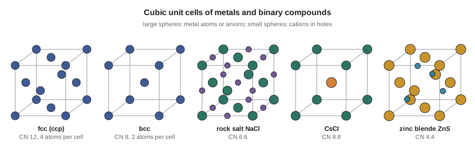
Many metals behave, to a good approximation, like hard spheres packed as tightly as possible. In one layer, each sphere touches six others in a hexagonal pattern. A second layer sits in half the hollows of the first. The third layer has a choice: it can lie directly over the first, giving the stacking sequence ABAB… of hexagonal close packing (hcp), or over the hollows of the first layer not covered by the second, giving ABCABC… This second sequence is cubic close packing (ccp), and its unit cell is the face-centered cube. In both arrangements each sphere has 12 nearest neighbors and the spheres fill 74.05 % of the space, the maximum possible for equal spheres, as Johannes Kepler conjectured in 1611 and Thomas Hales finally proved, with computer help, in 1998.
Magnesium, zinc and titanium are hcp; copper, silver, gold, aluminum and nickel are ccp. Many other metals, including iron at room temperature, sodium and chromium, adopt the slightly less dense body-centered cubic structure, in which each atom has 8 nearest neighbors and 6 more only 15 % farther away, filling 68 % of space. Iron changes from bcc to fcc at 912 °C and back to bcc at 1394 °C; the fcc form dissolves much more carbon in its holes, which is the basis of the heat treatment of steel.
Holes in close-packed structures
Close-packed arrays contain two kinds of holes, or interstices. An octahedral hole is surrounded by six spheres at the corners of an octahedron; a tetrahedral hole by four. In a close-packed array of N spheres there are N octahedral holes and 2N tetrahedral holes. In the fcc cell, the octahedral holes are at the center of the cube and the midpoints of the twelve edges (12 × ¼ + 1 = 4 per cell, one per atom), and the eight tetrahedral holes lie inside the cube at the centers of its eight small octants.
Simple geometry gives the largest sphere that fits in each hole without pushing the packed spheres apart. For spheres of radius r, an octahedral hole holds a sphere of radius 0.414r and a tetrahedral hole one of 0.225r. Hydrogen, carbon and nitrogen atoms can occupy holes in metals to form interstitial hydrides, carbides and nitrides such as PdHₓ and TiC, which are often very hard and have high melting points.
Ionic structures and the radius ratio
Many ionic solids can be described as a close-packed array of the larger ions, usually the anions, with the smaller cations in some or all of the holes. The main structure types are:
| Structure | Description | Coordination (cation:anion) | Examples |
|---|---|---|---|
| Rock salt (NaCl) | ccp anions, cations in all octahedral holes | 6:6 | NaCl, KBr, MgO, CaO, AgCl, FeO |
| Cesium chloride | Simple cubic anions, cation in the cube center | 8:8 | CsCl, CsBr, CsI, NH₄Cl |
| Zinc blende (sphalerite) | ccp anions, cations in half the tetrahedral holes | 4:4 | ZnS, CuCl, GaAs, Si (all atoms the same) |
| Wurtzite | hcp anions, cations in half the tetrahedral holes | 4:4 | ZnS, ZnO, GaN, AlN |
| Fluorite | ccp cations, anions in all tetrahedral holes | 8:4 | CaF₂, UO₂, ZrO₂ (cubic form) |
| Antifluorite | ccp anions, cations in all tetrahedral holes | 4:8 | Li₂O, Na₂O, K₂S |
| Rutile | Distorted hcp anions, cations in half the octahedral holes | 6:3 | TiO₂, SnO₂, MgF₂ |
| Perovskite | ABX₃: large A and X form ccp, B in octahedral holes | B 6, A 12 | CaTiO₃, BaTiO₃, SrTiO₃ |
Which structure a binary salt adopts depends largely on the radius ratio ρ = r₊/r₋. A cation is most stable when it touches all its anion neighbors; if it is too small for its hole it 'rattles', and a structure with a lower coordination number becomes better. The limiting ratios follow from geometry: 0.225 for tetrahedral (CN 4), 0.414 for octahedral (CN 6) and 0.732 for cubic (CN 8) coordination. So salts with ρ above 0.732 are predicted to adopt the CsCl structure, those between 0.414 and 0.732 the rock-salt structure, and those between 0.225 and 0.414 the zinc blende or wurtzite structure.
Worked problem
Using the radius ratio
Predict the structures of NaCl (r₊ = 102, r₋ = 181 pm), CsCl (167, 181), ZnS (74, 184) and LiI (76, 220).
Show solution
- NaCl: ρ = 0.56, between 0.414 and 0.732, so octahedral coordination: rock salt. Correct.
- CsCl: ρ = 0.92 > 0.732, so cubic coordination: cesium chloride structure. Correct.
- ZnS: ρ = 0.40, just below 0.414: tetrahedral coordination, zinc blende or wurtzite. Correct (both forms exist).
- LiI: ρ = 0.35 predicts tetrahedral coordination, but LiI has the rock-salt structure.
Answer: The radius ratio works for NaCl, CsCl and ZnS but fails for LiI. It also fails for many salts with covalent character; it is a guide, not a law. Only about half of the alkali halides, for example, are predicted correctly.
The radius ratio fails for several reasons: ions are not hard spheres, their radii depend on coordination number, covalent bonding favors lower coordination numbers (ZnS is tetrahedral partly because Zn–S bonds have strong covalent character), and the energy differences between structures are small. A more reliable approach compares lattice energies directly. The Madelung constants show that higher coordination gives a somewhat larger electrostatic energy (rock salt 1.748, CsCl 1.763, zinc blende 1.638, wurtzite 1.641, fluorite 2.519), but the gain is small, so other factors easily tip the balance. A structure map, plotting known compounds against properties such as electronegativity difference and average principal quantum number, separates the structure types more cleanly, an approach developed by John Mooser and William Pearson in 1959.
Calculating the Madelung constant
The Madelung sum for NaCl, introduced in lesson 3, converges so slowly that summing over spheres of increasing radius gives nonsense; the partial sums oscillate wildly. Harald Evjen showed in 1932 that summing over neutral cubes, counting ions on faces, edges and corners with weights ½, ¼ and ⅛ so that each cube carries no net charge, converges rapidly. The code below applies Evjen's method, then calculates densities, packing fractions, radius ratios and the intrinsic carrier concentrations of semiconductors discussed later in this lesson.
import math
# 1. Madelung constant of NaCl by Evjen's method (neutral cubes)
def evjen(n):
    total = 0.0
    for i in range(-n, n + 1):
        for j in range(-n, n + 1):
            for k in range(-n, n + 1):
                if i == j == k == 0:
                    continue
                w = 1.0
                for c in (i, j, k):
                    if abs(c) == n:
                        w *= 0.5          # face 1/2, edge 1/4, corner 1/8
                sign = -1 if (i + j + k) % 2 else 1
                total += -sign * w / math.sqrt(i * i + j * j + k * k)
    return total
for n in (1, 2, 3, 4, 6):
    print(f'Evjen cube n = {n}: A = {evjen(n):.5f}')

# 2. Densities from unit cells: rho = Z M / (N_A a^3)
NA = 6.02214e23
cells = [('NaCl rock salt', 4, 58.44, 564.0), ('CsCl', 1, 168.36, 412.3), ('Cu fcc', 4, 63.55, 361.5),
         ('Fe bcc', 2, 55.85, 286.6), ('Si diamond', 8, 28.086, 543.1)]
for name, Z, M, a in cells:
    rho = Z * M / (NA * (a * 1e-10) ** 3)
    print(f'{name:15} a = {a:6.1f} pm   density = {rho:5.2f} g/cm3')

# 3. Packing fractions of hard spheres
print('packing fractions: simple cubic %.4f, bcc %.4f, fcc/hcp %.4f, diamond %.4f' % (
    math.pi / 6, math.pi * math.sqrt(3) / 8, math.pi / (3 * math.sqrt(2)), math.pi * math.sqrt(3) / 16))

# 4. Radius ratio limits and predictions
print('limits: tetrahedral %.3f, octahedral %.3f, cubic %.3f' % (math.sqrt(3 / 2) - 1, math.sqrt(2) - 1, math.sqrt(3) - 1))
def predict(rp, rm):
    p = rp / rm
    return p, ('CN 8 (CsCl)' if p > 0.732 else 'CN 6 (rock salt)' if p > 0.414 else 'CN 4 (zinc blende)' if p > 0.225 else 'CN 3')
for salt, rp, rm, actual in [('NaCl', 102, 181, 6), ('CsCl', 167, 181, 8), ('ZnS', 74, 184, 4), ('LiI', 76, 220, 6), ('MgO', 72, 140, 6)]:
    p, pred = predict(rp, rm)
    print(f'{salt:5} ratio {p:.2f}: predicted {pred:20} observed CN {actual}')

# 5. Intrinsic carrier concentration n_i = sqrt(Nc Nv) exp(-Eg / 2kT), fixed gap
k = 8.617e-5   # eV/K
semis = {'Ge': (0.66, 1.04e19, 6.0e18), 'Si': (1.12, 2.8e19, 1.04e19), 'GaAs': (1.42, 4.7e17, 7.0e18)}
for T in (250, 300, 400):
    row = []
    for s, (Eg, Nc, Nv) in semis.items():
        f = (T / 300) ** 1.5
        ni = math.sqrt(Nc * f * Nv * f) * math.exp(-Eg / (2 * k * T))
        row.append(f'{s} {ni:.1e}')
print(f'T = {T} K: n_i (per cm3) ' + ', '.join(row))Evjen cube n = 1: A = 1.45603 Evjen cube n = 2: A = 1.75177 Evjen cube n = 3: A = 1.74704 Evjen cube n = 4: A = 1.74772 Evjen cube n = 6: A = 1.74760 NaCl rock salt a = 564.0 pm density = 2.16 g/cm3 CsCl a = 412.3 pm density = 3.99 g/cm3 Cu fcc a = 361.5 pm density = 8.94 g/cm3 Fe bcc a = 286.6 pm density = 7.88 g/cm3 Si diamond a = 543.1 pm density = 2.33 g/cm3 packing fractions: simple cubic 0.5236, bcc 0.6802, fcc/hcp 0.7405, diamond 0.3401 limits: tetrahedral 0.225, octahedral 0.414, cubic 0.732 NaCl ratio 0.56: predicted CN 6 (rock salt) observed CN 6 CsCl ratio 0.92: predicted CN 8 (CsCl) observed CN 8 ZnS ratio 0.40: predicted CN 4 (zinc blende) observed CN 4 LiI ratio 0.35: predicted CN 4 (zinc blende) observed CN 6 MgO ratio 0.51: predicted CN 6 (rock salt) observed CN 6 T = 250 K: n_i (per cm3) Ge 1.3e+12, Si 6.7e+07, GaAs 6.7e+03 T = 300 K: n_i (per cm3) Ge 2.3e+13, Si 6.7e+09, GaAs 2.1e+06 T = 400 K: n_i (per cm3) Ge 8.5e+14, Si 2.3e+12, GaAs 3.2e+09
Evjen's sums converge to 1.7476 within a few cubes. The densities agree with measured values (NaCl 2.165, Cu 8.96, Fe 7.87, Si 2.33 g/cm³), confirming the structures. The packing fractions show why bcc metals are slightly less dense than they would be in close packing, and why diamond-structure silicon is a very open solid, filling only 34 % of space. The radius-ratio predictions reproduce the worked example, including the failure for LiI.
From molecular orbitals to bands
Molecular orbital theory explains bonding in solids as well as in molecules. Two atoms each with one s orbital give one bonding and one antibonding MO. Three atoms in a row give three MOs, four give four, and N atoms give N molecular orbitals, spread over a range of energy whose width depends on the overlap between neighbors. When N is of order 10²³, the orbitals are so close together that they form a practically continuous band of allowed energies. The s orbitals of the atoms form an s band, the p orbitals a p band, and between bands there may be band gaps, ranges of energy with no orbitals at all.
Whether a solid conducts electricity depends on how the bands are filled. Electrons can carry current only if there are empty orbitals at energies just above the filled ones, so that an applied field can move them into states of slightly higher momentum. In a metal, the highest occupied band is only partly filled: sodium has one 3s electron per atom, so its s band, which can hold two per atom, is exactly half full. The energy of the highest filled level at absolute zero is called the Fermi level, and in a metal it lies inside a band. Magnesium, with two 3s electrons, would have a full s band and be an insulator, except that its s and p bands overlap, so electrons spill into the p band and both are partly filled.
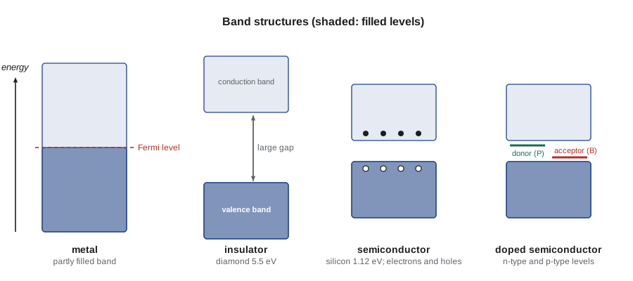
In an insulator, the highest occupied band, the valence band, is completely full and separated from the next empty band, the conduction band, by a large gap. Diamond's gap is about 5.5 eV, far too large for thermal energy (kT ≈ 0.026 eV at room temperature) to promote electrons across it, so diamond is an excellent insulator and is colorless, because visible photons (1.7 to 3.1 eV) cannot be absorbed. In a semiconductor the gap is small enough, roughly 0.1 to 3 eV, for some electrons to be excited thermally into the conduction band. Each excited electron leaves behind a vacancy in the valence band, a hole, which also carries current as neighboring electrons move into it. Silicon (1.12 eV), germanium (0.66 eV) and gallium arsenide (1.42 eV) are the classic semiconductors.
Semiconductors and doping
In a pure, or intrinsic, semiconductor, the concentration of electrons in the conduction band equals that of holes, n_i, which depends exponentially on the gap and temperature:
where N_c and N_v are effective densities of states that grow as T^(3/2). Because of the exponential, the conductivity of a semiconductor rises steeply with temperature, the opposite of a metal, whose conductivity falls as lattice vibrations scatter the electrons more. The calculation in the code shows that for silicon n_i is about 10¹⁰ per cm³ at room temperature (the simple fixed-gap model gives 7 × 10⁹), tiny compared with the 5 × 10²² silicon atoms per cm³. Germanium, with its smaller gap, has several thousand times more carriers, and n_i of every semiconductor rises by orders of magnitude between 250 and 400 K.
Pure silicon is therefore a poor conductor, and its usefulness comes from doping: adding tiny, controlled amounts of impurities. Replacing a few silicon atoms by phosphorus, which has five valence electrons, gives one extra electron per phosphorus that is only weakly bound (about 0.045 eV below the conduction band) and easily freed. This is an n-type semiconductor, with negative charge carriers. Replacing silicon by boron, with three valence electrons, creates an acceptor level just above the valence band; electrons from the valence band are easily promoted into it, leaving mobile holes. This is a p-type semiconductor. At a doping level of one phosphorus per million silicon atoms, the carrier concentration rises to about 5 × 10¹⁶ per cm³, millions of times the intrinsic value.
Joining p-type and n-type regions gives a p–n junction, which conducts in one direction only (a diode). The transistor, invented at Bell Laboratories by John Bardeen and Walter Brattain in December 1947 using germanium, with the junction transistor described by William Shockley soon after, launched the electronics revolution; the three shared the Nobel Prize in Physics in 1956. In a light-emitting diode, electrons and holes recombine at the junction and emit light with energy close to the band gap: GaAs emits in the infrared, GaP in green and GaN in blue. Solar cells work the other way round, absorbing photons with energy above the gap to create electron–hole pairs that the junction separates. Silicon, with a gap of 1.12 eV, absorbs most of the solar spectrum, and silicon cells dominate the market, while lead halide perovskites, ABX₃ materials first used in solar cells in 2009, are being developed for cheaper and more efficient devices.
Bringing the course together
Look back at what the principles of this course explain about solids. Atomic radii and effective nuclear charge (lesson 2) set ion sizes and the radius ratio. Lattice energies and the Madelung constant (lesson 3) explain why ionic solids form and which structures they prefer. Covalent bonding and hybridization (lesson 4) explain why silicon, germanium and zinc sulfide are tetrahedral. Symmetry (lessons 5 and 6) underlies the space groups that describe every crystal. Molecular orbital theory (lesson 7) becomes band theory. Hard–soft ideas (lesson 8) explain why ZnS and CdS are covalent semiconductors while MgO is an ionic insulator. Redox chemistry (lesson 9) governs batteries built from solid electrodes such as LiCoO₂ and graphite. The main-group survey (lessons 10 and 11) supplied the elements, from silicon to gallium nitride. CHEM-341 Inorganic Chemistry II takes these ideas into the d-block, where partly filled d orbitals add color, magnetism and catalysis, and CHEM-421 Materials Chemistry develops the chemistry of functional solids further.
Common mistakes
MistakeBody-centered cubic is a close-packed structure.
InsteadOnly ccp (fcc) and hcp are close packed (74 %); bcc fills 68 % of space.
MistakeA close-packed array has one hole of each kind per sphere.
InsteadIt has one octahedral and two tetrahedral holes per sphere.
MistakeThe radius ratio always predicts the structure.
InsteadIt fails often, as for LiI; covalency and small energy differences matter.
MistakeA larger Madelung constant always decides the structure.
InsteadDifferences between structures are small, and repulsion and covalency can outweigh them.
MistakeSemiconductors conduct less as they warm up, like metals.
InsteadTheir carrier concentration rises exponentially with temperature, so conductivity increases.
MistakeDoping with boron adds electrons to silicon.
InsteadBoron creates acceptor levels and holes: p-type. Phosphorus adds electrons: n-type.
Summary and key terms
- Crystals are described by lattices, bases and unit cells; atoms on corners, edges and faces are shared; ρ = ZM/(N_A a³).
- Close packing (hcp, ccp) fills 74 % of space with 12 neighbors; bcc fills 68 %; close-packed arrays have one octahedral and two tetrahedral holes per sphere.
- Ionic structures are anion arrays with cations in holes: rock salt, CsCl, zinc blende, wurtzite, fluorite, rutile and perovskite.
- The radius ratio (limits 0.225, 0.414, 0.732) is a rough guide to coordination; Madelung constants differ only slightly between structures.
- Band theory extends MO theory to solids: metals have partly filled bands, insulators a large gap and semiconductors a small one.
- Doping makes n-type and p-type semiconductors whose junctions give diodes, transistors, LEDs and solar cells.
- Unit cell
- The smallest repeating box from which a crystal can be built by translation.
- Coordination number
- The number of nearest neighbors of an atom or ion in a structure.
- Close packing
- An arrangement of equal spheres filling the maximum possible fraction of space, 74 %.
- Radius ratio
- The ratio r₊/r₋ of cation to anion radius used to predict coordination number.
- Band gap
- The energy range between the top of the valence band and the bottom of the conduction band.
- Fermi level
- The energy of the highest occupied electronic level at absolute zero.
- Doping
- Adding small controlled amounts of impurity atoms to a semiconductor to change its carrier concentration.
Practice problems
Work each problem on paper first, then reveal the answer to check.
Silver is fcc with a = 408.6 pm. Calculate its density (M = 107.87 g/mol).
Show answer
ρ = 4 × 107.87/(6.022 × 10²³ × (4.086 × 10⁻⁸ cm)³) = 10.50 g/cm³.
How many formula units are in the unit cell of fluorite, CaF₂, and why?
Show answer
Four: Ca²⁺ forms an fcc array (4 per cell) and F⁻ fills all 8 tetrahedral holes.
Predict the coordination of Mg²⁺ in MgO using r(Mg²⁺) = 72 and r(O²⁻) = 140 pm.
Show answer
ρ = 0.51: octahedral, rock-salt structure, as observed.
Calculate the largest radius ratio for a cation in a tetrahedral hole.
Show answer
√(3/2) − 1 = 0.225.
Why is diamond transparent while silicon is opaque and gray?
Show answer
Diamond's gap (5.5 eV) exceeds visible photon energies; silicon's gap (1.12 eV) lets it absorb all visible light.
Would arsenic or gallium make silicon n-type?
Show answer
Arsenic, with five valence electrons, donates an electron: n-type. Gallium gives p-type.
Lesson quiz · 5 questions
Score 60% or more to complete this lesson.
Create a free account to save your progress, take quizzes and earn a certificate.