
PHYS-410 · Lesson 9 of 12 · 21 min
Band theory: tight binding, metals, insulators and semiconductors
Lesson 8 built bands from free electrons perturbed by a weak lattice potential. This lesson starts from the opposite limit: electrons bound tightly to individual atoms, which can occasionally hop to neighbouring atoms. Both pictures lead to the same conclusion, that electron energies form bands separated by gaps, and the tight-binding picture is often closer to reality for the narrow \(d\) bands of transition metals, the bands of insulators and the \(\pi\) bands of graphene. The lesson then uses band filling to answer the question posed in lesson 1: why some solids are metals and others insulators. It closes with two ideas needed for lesson 10, the effective mass of an electron near a band edge and the concept of a hole.
From atoms to bands
Imagine bringing \(N\) identical atoms together from far apart. When they are isolated, each has the same set of energy levels, so each level is \(N\)-fold degenerate. As they approach, their outer orbitals overlap, and the degeneracy splits, just as two coupled pendulums with the same frequency acquire two normal-mode frequencies. With \(N\) atoms, each atomic level spreads into \(N\) closely spaced levels: a band. The width of the band is set by the overlap between neighbouring orbitals, so inner core levels, which barely overlap, form extremely narrow bands that remain essentially atomic, while the outer valence levels form wide bands. In the hydrogen molecule ion of PHYS-373, two atoms produced a bonding and an antibonding orbital; tight binding is the same idea extended to an infinite periodic array.
The tight-binding model
Consider a crystal with one atom per primitive cell and one atomic orbital per atom, \(\phi(\mathbf r)\), with energy \(E_0\). Build Bloch states as combinations of orbitals on all the atoms,
which satisfies Bloch's theorem by construction: shifting \(\mathbf r\) by a lattice vector relabels the sum and multiplies it by \(e^{i\mathbf k\cdot\mathbf R}\). This is the linear combination of atomic orbitals (LCAO) used in chemistry, organized by the lattice symmetry. Its energy is \(E(\mathbf k) = \langle\psi_{\mathbf k}|H|\psi_{\mathbf k}\rangle\). Keeping only the matrix elements between an orbital and itself, \(E_0\) (absorbing a small crystal-field shift), and between closest neighbours, \(-t\) with \(t > 0\) called the hopping integral, and neglecting the overlap of orbitals on different atoms, gives
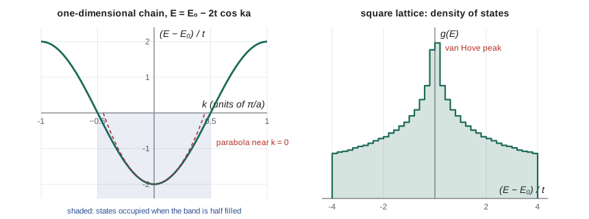
where the sum runs over the vectors \(\boldsymbol\delta\) to the closest neighbours. For a chain with spacing \(a\), the two neighbours at \(\pm a\) give
a band of width \(4t\) centred on the atomic energy. For a simple cubic lattice, \(E = E_0 - 2t(\cos k_xa + \cos k_ya + \cos k_za)\), width \(12t\). In general the bandwidth is \(2zt\), where \(z\) is the coordination number. Wide bands come from large overlap and many neighbours. The hopping integral falls roughly exponentially with distance between atoms, which is why compressing a solid broadens its bands, and why under extreme pressure many insulators become metals.
Effective mass
Near the bottom of the chain's band, at \(k = 0\), expand the cosine: \(E \approx E_0 - 2t + ta^2k^2\). This is the free-electron parabola, \(\hbar^2k^2/2m^*\), with an effective mass
In general, near a band minimum or maximum, the effective mass is defined by the curvature, \(1/m^* = \hbar^{-2}\,d^2E/dk^2\). Narrow bands, with small \(t\), give heavy electrons; wide bands give light ones. The effective mass is not just a fudge factor: in an applied force, a wave packet built from states near the band edge accelerates as if it had mass \(m^*\), because the lattice exerts forces on it that the effective mass absorbs. In semiconductors, measured effective masses are often much smaller than the free mass: \(0.067m\) for electrons in gallium arsenide, \(0.19m\) and \(0.98m\) (depending on direction) for electrons in silicon. Near the top of a band, the curvature is negative and so is \(m^*\): an electron there accelerates opposite to the applied force. That oddity is resolved by the hole picture below.
Density of states
The density of states \(g(E)\), the number of states per unit energy, determines how many electrons sit near any energy, and therefore heat capacities, optical absorption and the position of the Fermi level. For a band \(E(\mathbf k)\) it is found by counting how many allowed \(\mathbf k\) values fall in each energy interval. The program does exactly that for the square lattice, sampling 360,000 points in the zone. The result has steps at the band edges, as for any two-dimensional parabolic band, and a peak at the centre, \(E = E_0\), where the constant-energy contour passes through the saddle points at \(X = (\pi/a, 0)\), where the gradient of \(E\) vanishes. These van Hove singularities have the same origin as the phonon peaks of lesson 5. When the Fermi level lies near such a peak, many electrons are available for scattering and pairing, and in some materials this is linked to magnetism or superconductivity.
import math
# Tight binding: one s orbital per site, hopping t between nearest atoms.
t, a = 1.0, 1.0
print("1D chain: E(k) = E0 - 2 t cos(ka), bandwidth 4t")
for frac in (0, 0.25, 0.5, 0.75, 1):
    k = frac * math.pi / a
    print(f"  k = {frac:4.2f} pi/a : E - E0 = {-2 * t * math.cos(k * a):+.4f} t")
print("  effective mass at the band bottom: m* = hbar^2 / (2 t a^2); halving t doubles m*")
print()
# 2D square lattice: E = -2t (cos kx a + cos ky a); density of states by sampling the zone
N = 600
bins = 24
hist = [0] * bins
for i in range(N):
    for j in range(N):
        kx = -math.pi + 2 * math.pi * (i + 0.5) / N
        ky = -math.pi + 2 * math.pi * (j + 0.5) / N
        E = -2 * t * (math.cos(kx) + math.cos(ky))
        hist[min(int((E + 4) / 8 * bins), bins - 1)] += 1
print("2D square lattice DOS (energy at mid-bin in units of t : relative weight)")
peak = max(hist)
for b in range(0, bins, 2):
    Emid = -4 + 8 * (b + 0.5) / bins
    print(f"  {Emid:+5.2f} : {'#' * round(40 * hist[b] / peak)}")
print("  the DOS is a step at the band edges and diverges logarithmically at E = 0 (van Hove singularity)")
print()
# Counting electrons: a band holds 2 electrons per primitive cell
for name, electrons, bands in (("Na (1 valence electron)", 1, "half-filled band: metal"),
                                ("Mg (2 valence electrons)", 2, "filled band, but bands overlap: metal"),
                                ("Si (8 per primitive cell)", 8, "4 filled bands, gap 1.12 eV: semiconductor"),
                                ("diamond (8 per primitive cell)", 8, "4 filled bands, gap 5.5 eV: insulator")):
print(f" {name:32s} {electrons / 2:4.1f} bands' worth -> {bands}")1D chain: E(k) = E0 - 2 t cos(ka), bandwidth 4t k = 0.00 pi/a : E - E0 = -2.0000 t k = 0.25 pi/a : E - E0 = -1.4142 t k = 0.50 pi/a : E - E0 = -0.0000 t k = 0.75 pi/a : E - E0 = +1.4142 t k = 1.00 pi/a : E - E0 = +2.0000 t effective mass at the band bottom: m* = hbar^2 / (2 t a^2); halving t doubles m* 2D square lattice DOS (energy at mid-bin in units of t : relative weight) -3.83 : ############# -3.17 : ############## -2.50 : ################ -1.83 : ################## -1.17 : ###################### -0.50 : ############################ +0.17 : ######################################## +0.83 : ######################## +1.50 : #################### +2.17 : ################# +2.83 : ############### +3.50 : ############## the DOS is a step at the band edges and diverges logarithmically at E = 0 (van Hove singularity) Na (1 valence electron) 0.5 bands' worth -> half-filled band: metal Mg (2 valence electrons) 1.0 bands' worth -> filled band, but bands overlap: metal Si (8 per primitive cell) 4.0 bands' worth -> 4 filled bands, gap 1.12 eV: semiconductor diamond (8 per primitive cell) 4.0 bands' worth -> 4 filled bands, gap 5.5 eV: insulator
Metals, insulators and semiconductors
Each band holds \(2N\) electrons, two per primitive cell, as lesson 8 showed. The ground state is found by filling the lowest bands with the available valence electrons, and the electrical character of the crystal follows at once.
If some band is only partly filled, the highest occupied states lie in the middle of a band, with empty states immediately above them. An applied field can shift electrons into those empty states, producing a current: the crystal is a metal. Sodium, with one valence electron per primitive cell, half fills its band. Copper, silver and gold, with one \(s\) electron beyond a filled \(d\) shell, also have a half-filled band.
If the valence electrons exactly fill some number of bands, and a gap separates the highest filled band from the next, then at zero temperature no electron can move into a nearby state. A completely filled band carries no current, because for every electron with velocity \(\mathbf v\) there is one with \(-\mathbf v\), and a field cannot change this. The crystal is an insulator. This requires an even number of electrons per primitive cell, which is why diamond, with 8 valence electrons per two-atom cell, can be an insulator. Whether such a crystal behaves as an insulator or a semiconductor at room temperature depends on the size of the gap. Diamond's 5.5 eV gap means essentially no electrons are thermally excited; silicon's 1.12 eV and germanium's 0.66 eV are small enough that some are, and their conductivity rises steeply with temperature, as lesson 10 explores. Alan Wilson set out this classification in 1931, and it explained for the first time why the electrical properties of solids differ so enormously.
An even electron count is necessary but not sufficient for an insulator. Magnesium, calcium and zinc have two valence electrons per primitive cell, yet they are metals. In three dimensions, bands can overlap in energy: the bottom of the second band at one point of the zone lies below the top of the first at another. Electrons then spill into the second band, leaving the first slightly empty, and both are partly filled. Such materials have small numbers of electrons and holes and are sometimes called semimetals when the overlap is small, as in bismuth and graphite.
The simple counting rule fails in another way when electrons repel each other strongly. Nickel oxide has an odd number of electrons per cell in the relevant \(d\) band and should, by band theory, be a metal. It is a good insulator. Nevill Mott argued in 1937 and 1949 that when the Coulomb energy of putting two electrons on the same atom exceeds the bandwidth, electrons localize one per atom, and the crystal becomes a Mott insulator. Mott insulators, beyond the independent-electron picture of this course, include the parent compounds of the copper oxide superconductors of lesson 12.
Holes
Consider a band that is completely full except for one empty state, at wave vector \(\mathbf k_e\). The total crystal momentum and current of the full band are zero, so the band with one electron missing carries current and momentum equal and opposite to those of the missing electron. It behaves exactly like a single particle with positive charge \(+e\), crystal momentum \(-\hbar\mathbf k_e\), and, near the top of the band where the electron's effective mass is negative, a positive effective mass. This fictitious particle is a hole. Holes explain the positive Hall coefficients of lesson 7: in aluminium, beryllium and zinc, some carriers lie in nearly full regions of a band and respond to fields as positive charges. In semiconductors, the holes left in the valence band when electrons are excited across the gap carry current alongside the electrons, and holes introduced by doping are the majority carriers in p-type material in lesson 10.
Worked problem
Bandwidth and effective mass
In a tight-binding chain with spacing \(a = 0.3\) nm, the hopping integral is \(t = 1.0\) eV. Find the bandwidth and the effective mass at the band bottom in units of the free-electron mass.
Show solution
- Bandwidth \(4t = 4.0\) eV.
- \(m^* = \hbar^2/(2ta^2) = (1.055 \times 10^{-34})^2/(2 \times 1.602 \times 10^{-19} \times 9 \times 10^{-20}) = 3.86 \times 10^{-31}\) kg.
- \(m^*/m = 3.86 \times 10^{-31}/9.11 \times 10^{-31} = 0.42\).
Answer: A 4.0 eV band with \(m^* \approx 0.42m\); halving \(t\) would double \(m^*\) and halve the bandwidth.
Common mistakes
MistakeAssuming every crystal with an even number of electrons per cell is an insulator.
InsteadBands can overlap, as in magnesium and zinc.
MistakeThinking a filled band can carry current.
InsteadVelocities cancel in pairs; a field cannot change a full band.
MistakeTreating the effective mass as a property of the electron itself.
InsteadIt describes the band curvature and differs between materials and bands.
MistakeDescribing a hole as a missing positive charge.
InsteadA hole is a missing electron and behaves as a positive charge with positive mass near a band top.
MistakeUsing band theory for strongly correlated materials without question.
InsteadMott insulators such as NiO are insulating despite partly filled bands.
Summary and key terms
- Tight binding: \(\psi_{\mathbf k} = N^{-1/2}\sum e^{i\mathbf k\cdot\mathbf R}\phi(\mathbf r - \mathbf R)\) gives \(E = E_0 - t\sum e^{i\mathbf k\cdot\boldsymbol\delta}\), a band of width \(2zt\).
- Near a band extremum, \(1/m^* = \hbar^{-2}d^2E/dk^2\); for a chain \(m^* = \hbar^2/(2ta^2)\).
- The density of states has van Hove singularities where \(\nabla_{\mathbf k}E = 0\).
- Partly filled bands give metals; filled bands with a gap give insulators or, for small gaps, semiconductors; overlapping bands give metals or semimetals.
- A nearly full band behaves as a set of holes with charge \(+e\); strong repulsion can make a Mott insulator.
- Tight-binding model
- Bands built from atomic orbitals with hopping between neighbours.
- Hopping integral
- The matrix element \(-t\) of the Hamiltonian between orbitals on neighbouring atoms.
- Effective mass
- The mass \(m^*\) defined by the band curvature near an extremum.
- Hole
- The quasiparticle describing an empty state in a nearly full band.
- Mott insulator
- An insulator caused by electron repulsion rather than by band filling.
Practice problems
Work each problem on paper first, then reveal the answer to check.
What is the bandwidth of a tight-binding fcc crystal in terms of \(t\)?
Show answer
\(2zt = 24t\).
A 1D tight-binding band holds one electron per atom. Where is the Fermi level?
Show answer
At \(E_0\), with \(k_F = \pi/2a\); the band is half full and the solid is a metal.
Find \(m^*\) at the top of the chain band, \(k = \pi/a\).
Show answer
\(E \approx E_0 + 2t - ta^2(k - \pi/a)^2\), so \(m^* = -\hbar^2/(2ta^2)\).
Why is calcium, with two valence electrons per cell, a metal?
Show answer
Its \(s\) and \(p\) bands overlap in energy, so both are partly filled.
Germanium has a gap of 0.66 eV. Classify it.
Show answer
A semiconductor: insulating at absolute zero but conducting appreciably at room temperature.
Lesson quiz · 5 questions
Score 60% or more to complete this lesson.
Create a free account to save your progress, take quizzes and earn a certificate.