
CMPUT-229 · Lesson 9 of 12 · 31 min
Processor design: the single-cycle datapath and control
You now know what RV32I instructions do and how they are encoded, and lesson 4 supplied the building blocks: registers, multiplexers, adders, an ALU and a register file. This lesson puts them together into a working processor. The design here, a single-cycle implementation, executes each instruction completely in one long clock cycle. No real high-performance processor works this way, but every real processor contains the same datapath, and pipelining, the subject of lesson 10, is easiest to understand as a way of overlapping the steps of this design. By the end of the lesson you will be able to trace any RV32I instruction through the datapath, state the value of every control signal, and work out the clock period from component delays.
The method follows the way processors are actually designed. First list what each class of instruction needs to do. Then assemble a datapath that can do all of it, adding multiplexers wherever two instructions need different inputs at the same point. Finally design the control unit, the combinational logic that looks at each instruction's opcode and function fields and sets every multiplexer and write enable accordingly.
What each instruction needs
Every instruction begins the same way. The processor fetches the instruction from memory at the address in the PC, and computes PC + 4, the address of the next instruction in sequence. After that, the classes diverge. R-type instructions read two registers, pass them through the ALU and write the result back to a register. I-type arithmetic does the same with an immediate in place of the second register. Loads compute an address with the ALU from a register and an immediate, read data memory and write the loaded value to a register. Stores compute an address the same way and write a register's value to data memory. Branches compare two registers and, if the condition holds, replace PC + 4 with PC plus a sign-extended offset. jal writes PC + 4 to rd and jumps to PC + offset; jalr writes PC + 4 to rd and jumps to rs1 + offset. lui writes an upper immediate to rd, and auipc writes PC plus an upper immediate.
| Class | Example | Register reads | ALU computes | Memory | Register write | Next PC |
|---|---|---|---|---|---|---|
| R-type | add rd, rs1, rs2 | rs1, rs2 | rs1 op rs2 | — | ALU result | PC + 4 |
| I-type ALU | addi rd, rs1, imm | rs1 | rs1 op imm | — | ALU result | PC + 4 |
| Load | lw rd, imm(rs1) | rs1 | rs1 + imm | Read | Loaded data | PC + 4 |
| Store | sw rs2, imm(rs1) | rs1, rs2 | rs1 + imm | Write rs2 | — | PC + 4 |
| Branch | beq rs1, rs2, off | rs1, rs2 | Comparison | — | — | PC + off if taken |
| jal | jal rd, off | — | — | — | PC + 4 | PC + off |
| jalr | jalr rd, imm(rs1) | rs1 | rs1 + imm | — | PC + 4 | ALU result |
| lui | lui rd, imm | — | imm (passed through) | — | imm | PC + 4 |
Reading down the table shows where the datapath needs choices. The ALU's second input is sometimes a register and sometimes an immediate, so a multiplexer selects it. The value written back to the register file is sometimes the ALU result, sometimes data from memory and sometimes PC + 4, so a three-input multiplexer selects it. The next PC is sometimes PC + 4, sometimes PC plus an offset and sometimes the ALU result, so another multiplexer selects that. Each choice becomes a control signal.
The datapath
The single-cycle datapath has these components. The PC is a 32-bit register. The instruction memory is read at the PC's address and outputs the 32-bit instruction; in this simple design it is separate from the data memory, so an instruction fetch and a data access can happen in the same cycle, an arrangement called a Harvard architecture at this level and approximated in real processors by separate instruction and data caches. The register file has two read ports, addressed directly by the rs1 and rs2 fields of the instruction, and one write port, addressed by rd. An immediate generator extracts the immediate from whichever format the instruction uses and sign-extends it to 32 bits. The ALU computes the arithmetic or logic result. The data memory is read or written at the address the ALU produces. Two adders compute PC + 4 and PC + immediate, and multiplexers route values between the units.
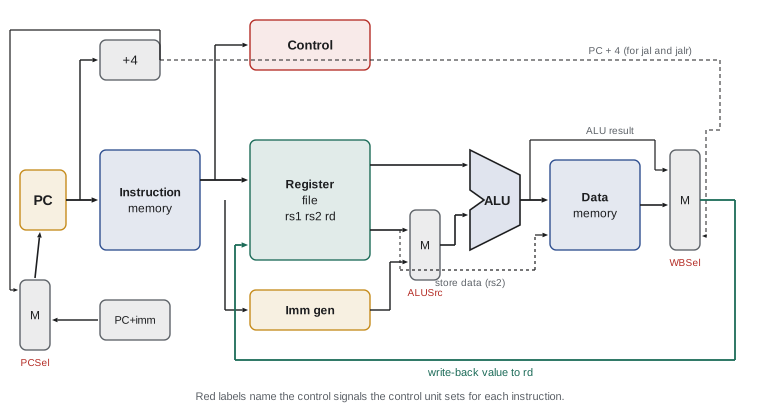
Because the register fields sit in the same place in every format, as lesson 5 emphasized, the register file can start reading rs1 and rs2 as soon as the instruction arrives, before the control unit has decided what the instruction is. If the instruction turns out not to use rs2, the value read is simply ignored. Reading registers speculatively like this costs nothing and saves time, and it is the payoff for the slightly awkward S and B formats.
The immediate generator is a good example of how the encoding shapes the hardware. It needs a multiplexer for each of the 32 output bits, choosing which instruction bit, or the sign bit, goes there according to the format. Because the RISC-V formats keep immediate bits in the same instruction positions whenever possible, and always take the sign from instruction bit 31, most output bits have only two or three possible sources, which keeps the generator small and fast.
Control
The control unit is combinational logic that takes the opcode, funct3 and funct7 fields and produces the control signals. In the design here, they are: RegWrite, which enables writing the register file; ALUSrc, which selects a register or the immediate as the ALU's second input; ALUOp, which tells the ALU what to compute; MemRead and MemWrite, which enable data memory; WBSel, which selects the value to write back; and PCSel, which selects the next PC. The branch decision combines a Branch signal from the control unit with the comparison result: the PC takes the branch target only when the instruction is a branch and its condition holds.
# Main control signals for each class of instruction (x = don't care)
SIGNALS = ['RegWrite', 'ALUSrc', 'ALUOp', 'MemRead', 'MemWrite', 'WBSel', 'PCSel']
CONTROL = {
    'R-type': (1, 'reg', 'funct', 0, 0, 'alu', 'pc+4'),
    'I-ALU':  (1, 'imm', 'funct', 0, 0, 'alu', 'pc+4'),
    'load':   (1, 'imm', 'add',   1, 0, 'mem', 'pc+4'),
    'store':  (0, 'imm', 'add',   0, 1, 'x',   'pc+4'),
    'branch': (0, 'reg', 'cmp',   0, 0, 'x',   'pc+imm if taken'),
    'jal':    (1, 'x',   'x',     0, 0, 'pc+4', 'pc+imm'),
    'jalr':   (1, 'imm', 'add',   0, 0, 'pc+4', 'alu'),
    'lui':    (1, 'imm', 'pass',  0, 0, 'alu', 'pc+4'),
}
print(f'{"class":<8}' + ''.join(f'{s:>9}' for s in SIGNALS[:-1]) + '  PCSel')
for cls, vals in CONTROL.items():
print(f'{cls:<8}' + ''.join(f'{str(v):>9}' for v in vals[:-1]) + f' {vals[-1]}')class RegWrite ALUSrc ALUOp MemRead MemWrite WBSel PCSel R-type 1 reg funct 0 0 alu pc+4 I-ALU 1 imm funct 0 0 alu pc+4 load 1 imm add 1 0 mem pc+4 store 0 imm add 0 1 x pc+4 branch 0 reg cmp 0 0 x pc+imm if taken jal 1 x x 0 0 pc+4 pc+imm jalr 1 imm add 0 0 pc+4 alu lui 1 imm pass 0 0 alu pc+4
Two features of the table matter. First, a write enable must never be a don't-care: a store with RegWrite accidentally set to 1 would corrupt a register, so RegWrite and MemWrite always have definite values. Second, many signals are don't-cares for some classes, and designers exploit them to simplify the logic, just as the sum-of-products simplification in lesson 4 did. In practice the main control unit produces a short ALUOp code, and a second, smaller block, the ALU control, combines ALUOp with funct3 and funct7 to choose the exact ALU operation: for an R-type instruction, funct3 = 000 with funct7 = 0000000 means add, and with funct7 = 0100000 means subtract. Splitting control into levels keeps each block small, a standard technique.
Worked problem
Tracing a load through the datapath
Trace lw t3, 8(s0) through the single-cycle datapath, assuming s0 = 0x10010000 and the word at 0x10010008 is 42.
Show solution
- Fetch: instruction memory outputs the lw word; the adder computes PC + 4.
- Decode and read: rs1 = s0, so read data 1 = 0x10010000; the immediate generator outputs 8; control sets RegWrite 1, ALUSrc imm, ALUOp add, MemRead 1, MemWrite 0, WBSel mem, PCSel pc+4.
- Execute: the ALU adds 0x10010000 + 8 = 0x10010008.
- Memory: data memory reads address 0x10010008 and outputs 42.
- Write back: the WBSel multiplexer chooses memory data, and at the clock edge 42 is written to t3 while the PC becomes PC + 4.
Answer: t3 = 42 after the clock edge. The load uses every major unit in sequence, which is why it is the slowest instruction in a single-cycle design.
A single-cycle simulator
The behaviour of the whole datapath fits in a short program. The simulator below executes real RV32I machine words, the encodings produced by the LLVM assembler for a nine-instruction program, and prints the value on each important wire in every cycle: the PC, the instruction, the register values read, the immediate, the ALU result, any memory access and the value written back. Each loop iteration is one clock cycle, and every state change, to registers, memory and the PC, happens together at the end of the iteration, exactly as at a clock edge.
PROGRAM = [0x00500293, 0x00700313, 0x006283B3, 0x00702023, 0x00002E03,
           0x406E0EB3, 0x005E8463, 0x00100F13, 0x00200F93]
NAMES = ['addi t0,zero,5', 'addi t1,zero,7', 'add t2,t0,t1', 'sw t2,0(zero)', 'lw t3,0(zero)',
         'sub t4,t3,t1', 'beq t4,t0,8', 'addi t5,zero,1', 'addi t6,zero,2']
ABI = {5: 't0', 6: 't1', 7: 't2', 28: 't3', 29: 't4', 30: 't5', 31: 't6'}
sext = lambda v, b: v - (1 << b) if v >> (b - 1) else v

def immediate(w, op):
    if op in (0x13, 0x03): return sext(w >> 20, 12)                       # I-type
    if op == 0x23: return sext(((w >> 25) << 5) | ((w >> 7) & 31), 12)    # S-type
    if op == 0x63:                                                         # B-type
        return sext(((w >> 31) << 12) | (((w >> 7) & 1) << 11) | (((w >> 25) & 63) << 5) | (((w >> 8) & 15) << 1), 13)
    return 0

reg, mem, pc = [0] * 32, {}, 0
while pc // 4 < len(PROGRAM):
    w = PROGRAM[pc // 4]
    op, rd, f3 = w & 0x7F, (w >> 7) & 31, (w >> 12) & 7
    rs1, rs2, f7 = (w >> 15) & 31, (w >> 20) & 31, w >> 25
    a, b, imm = reg[rs1], reg[rs2], immediate(w, op)             # register file read
    alu_b = b if op in (0x33, 0x63) else imm                      # ALUSrc multiplexer
    alu = a - alu_b if (op == 0x33 and f7 == 32) else a + alu_b   # ALU (add or sub here)
    wb, note, next_pc = None, '', pc + 4
    if op in (0x33, 0x13): wb = alu
    elif op == 0x03: wb = mem.get(alu, 0); note = f'read M[{alu}]={wb}'
    elif op == 0x23: note = f'write M[{alu}]={b}'
    elif op == 0x63:
        taken = a == b                                            # beq comparison
        note = 'taken' if taken else 'not taken'
        if taken: next_pc = pc + imm                              # PCSel multiplexer
    print(f'PC={pc:2d} {NAMES[pc // 4]:<15} rs1={a:3d} rs2={b:3d} imm={imm:3d} '
          f'ALU={alu:4d} {note:<14}' + (f'{ABI[rd]}<-{wb}' if wb is not None else ''))
    # clock edge: all state updates happen together
    if op == 0x23: mem[alu] = b
    if wb is not None and rd: reg[rd] = wb
    pc = next_pc
print('final:', {ABI[i]: reg[i] for i in ABI})PC= 0 addi t0,zero,5 rs1= 0 rs2= 0 imm= 5 ALU= 5 t0<-5
PC= 4 addi t1,zero,7 rs1= 0 rs2= 0 imm= 7 ALU= 7 t1<-7
PC= 8 add t2,t0,t1 rs1= 5 rs2= 7 imm= 0 ALU= 12 t2<-12
PC=12 sw t2,0(zero) rs1= 0 rs2= 12 imm= 0 ALU= 0 write M[0]=12
PC=16 lw t3,0(zero) rs1= 0 rs2= 0 imm= 0 ALU= 0 read M[0]=12 t3<-12
PC=20 sub t4,t3,t1 rs1= 12 rs2= 7 imm= 0 ALU= 5 t4<-5
PC=24 beq t4,t0,8 rs1= 5 rs2= 5 imm= 8 ALU= 10 taken
PC=32 addi t6,zero,2 rs1= 0 rs2= 0 imm= 2 ALU= 2 t6<-2
final: {'t0': 5, 't1': 7, 't2': 12, 't3': 12, 't4': 5, 't5': 0, 't6': 2}Follow the beq row: t4 = 12 − 7 = 5 equals t0, so the branch is taken and the PC jumps from 24 to 32, skipping the instruction that would have set t5. The final register values confirm it: t5 is still 0 and t6 is 2. Note also that in the beq row the ALU result is computed but nothing uses it; in the single-cycle design every unit computes something every cycle, and control decides which results matter.
Timing: why single-cycle is slow
In a single-cycle design, every instruction must finish within one clock period, so the period must be long enough for the slowest instruction. The slowest is the load, which uses every unit in sequence: instruction memory, register read, ALU, data memory, write-back multiplexer and register setup. An add, which skips data memory, could finish much sooner, but it still has to wait for the clock. The table of delays below is illustrative but realistic in its proportions, with memory accesses the slowest components.
# Illustrative component delays in picoseconds
D = {'imem': 250, 'regread': 150, 'mux': 25, 'alu': 200, 'dmem': 250, 'regsetup': 20}
paths = {
    'R-type': ['imem', 'regread', 'mux', 'alu', 'mux', 'regsetup'],
    'load':   ['imem', 'regread', 'mux', 'alu', 'dmem', 'mux', 'regsetup'],
    'store':  ['imem', 'regread', 'mux', 'alu', 'dmem'],
    'branch': ['imem', 'regread', 'mux', 'alu', 'mux'],
    'jal':    ['imem', 'mux', 'regsetup'],
}
times = {k: sum(D[c] for c in v) for k, v in paths.items()}
for k, t in times.items():
    print(f'{k:>6}: {t} ps')
period = max(times.values())
print(f'single-cycle clock period = {period} ps ({1e3 / period:.2f} GHz)')

mix = {'R-type': 0.44, 'load': 0.24, 'store': 0.12, 'branch': 0.16, 'jal': 0.04}
avg = sum(mix[k] * times[k] for k in mix)
print(f'average time actually needed per instruction = {avg:.0f} ps')
print(f'time wasted by the fixed clock = {100 * (1 - avg / period):.0f}%')R-type: 670 ps load: 920 ps store: 875 ps branch: 650 ps jal: 295 ps single-cycle clock period = 920 ps (1.09 GHz) average time actually needed per instruction = 736 ps time wasted by the fixed clock = 20%
The single-cycle design has a CPI of exactly 1, but its clock period is set by the load, and on average a fifth of every cycle is spent waiting. Worse, the problem grows with richer instruction sets: a floating-point divide would stretch every cycle for every instruction. Two classic responses exist. A multicycle design breaks each instruction into steps of one short cycle each, letting simple instructions take fewer cycles than complex ones, at the cost of a CPI above 1. A pipelined design, lesson 10's subject, also breaks instructions into steps but overlaps them, so that a new instruction starts every cycle. Pipelining wins, which is why essentially every processor since the late 1980s is pipelined.
Worked problem
Comparing single-cycle and multicycle designs
Using the delays above, a multicycle design has a 250 ps clock, the slowest single step. Loads take 5 cycles, stores and R-type 4, branches 3 and jal 3. Is it faster than the single-cycle design for the instruction mix above?
Show solution
- Single-cycle: one 920 ps cycle per instruction, so 920 ps on average.
- Multicycle CPI = 0.44 × 4 + 0.24 × 5 + 0.12 × 4 + 0.16 × 3 + 0.04 × 3 = 4.04.
- Average time = 4.04 × 250 ps = 1,010 ps.
Answer: The multicycle design is slower here, about 1,010 ps per instruction against 920 ps, because each step pays the full 250 ps even when it needs less. Multicycle designs pay off when instruction times vary widely; pipelining is the better answer for RISC-V.
Beyond the basic datapath
The design in this lesson omits several things a real processor needs. It has no way to handle exceptions, such as an illegal instruction or a misaligned access, or interrupts from devices; RISC-V handles these by saving the PC in a control and status register called mepc (or sepc in supervisor mode), recording the cause in mcause, and jumping to a handler address, as lesson 12 describes. It supports only word loads and stores; byte and halfword accesses need extra logic to select and extend bytes. And it treats memory as if every access took one cycle, which real memory, as lesson 11 shows, does not. Each extension adds multiplexers, control signals and states, but none changes the basic structure: fetch, decode and read registers, execute, access memory, write back.
| Signal | Purpose | Values |
|---|---|---|
| RegWrite | Enable writing rd at the clock edge | 1 for instructions that write a register |
| ALUSrc | Choose the ALU's second input | Register rs2 or immediate |
| ALUOp | Tell the ALU control what to compute | Add, compare, or use funct3 and funct7 |
| MemRead, MemWrite | Enable data memory reads or writes | Loads and stores |
| WBSel | Choose the write-back value | ALU result, memory data or PC + 4 |
| Branch / PCSel | Choose the next PC | PC + 4, PC + immediate, or rs1 + immediate |
Common mistakes
MistakeLeaving RegWrite or MemWrite as a don't-care for some instruction.
InsteadWrite enables must always have definite values; a stray write corrupts state.
MistakeThinking a CPI of 1 makes the single-cycle design fast.
InsteadIts clock period must cover the slowest instruction, usually a load, so every instruction pays that time.
MistakeAssuming the register file waits for decoding before reading.
InsteadBecause rs1 and rs2 are always in the same bits, registers are read in parallel with decoding and unused values ignored.
MistakeForgetting that branches need both a Branch control signal and the comparison result.
InsteadThe PC takes the target only when the instruction is a branch and its condition holds.
MistakeTreating jal and jalr as needing no register write.
InsteadBoth write the return address, PC + 4, to rd; the WBSel multiplexer needs a PC + 4 input.
Summary and key terms
- Every instruction begins by fetching from instruction memory at the PC and computing PC + 4.
- The datapath combines the PC, instruction and data memories, register file, immediate generator, ALU, adders and multiplexers.
- Multiplexers appear wherever instructions need different inputs: ALUSrc, WBSel and PCSel are the main ones.
- The control unit decodes opcode, funct3 and funct7 into control signals; a separate ALU control refines ALUOp.
- Fixed register field positions let the register file read operands in parallel with decoding.
- In a single-cycle design CPI = 1 but the clock period equals the slowest instruction's path, usually the load.
- Multicycle and pipelined designs split instructions into shorter steps; pipelining overlaps them and dominates in practice.
- Datapath
- The hardware that holds and transforms data: registers, ALU, memories, adders and multiplexers.
- Control unit
- The logic that decodes instructions and sets every multiplexer and write enable.
- Control signal
- A wire from the control unit selecting a multiplexer input or enabling a write.
- Immediate generator
- The block that extracts and sign-extends the immediate for each instruction format.
- ALU control
- A second-level decoder combining ALUOp with funct3 and funct7 to choose the ALU operation.
- Single-cycle implementation
- A design in which each instruction completes in one long clock cycle.
- Multicycle implementation
- A design that executes each instruction as a sequence of short clock cycles.
- Write enable
- A signal allowing a register or memory to change at the clock edge.
- Harvard architecture
- A design with separate instruction and data memories or paths.
- Don't-care
- A control value that does not affect the result for a given instruction, usable to simplify logic.
Practice problems
Work each problem on paper first, then reveal the answer to check.
Which control signals does sw t0, 4(sp) set?
Show answer
RegWrite 0, ALUSrc imm, ALUOp add, MemRead 0, MemWrite 1, WBSel don't-care, PCSel pc+4.
What value does the WBSel multiplexer choose for jal?
Show answer
PC + 4, the return address.
Why does the ALU need a multiplexer on its second input but not its first?
Show answer
The first input is always rs1 in this design; the second is rs2 for R-type and branches but the immediate for I-type, loads and stores.
Using the lesson's delays, what is the path delay for an R-type instruction?
Show answer
250 + 150 + 25 + 200 + 25 + 20 = 670 ps.
If data memory became 150 ps instead of 250 ps, what would the single-cycle period be?
Show answer
The load path would be 820 ps and the R-type 670 ps, so 820 ps.
What decides whether a beq changes the PC?
Show answer
The Branch control signal and the ALU or comparator result together: the PC takes the target only if both indicate a taken branch.
How does jalr compute its target?
Show answer
The ALU adds rs1 and the immediate; PCSel selects the ALU result as the next PC.
Why is RegWrite never a don't-care?
Show answer
Leaving it undefined might write garbage into a register for stores and branches.
What extra hardware does lb need compared with lw?
Show answer
Logic to select the right byte of the word and sign-extend it.
Why is a single-cycle design worse for an ISA with a slow divide instruction?
Show answer
The clock period would have to cover the divide, slowing every other instruction too.
Lesson quiz · 5 questions
Score 60% or more to complete this lesson.
Create a free account to save your progress, take quizzes and earn a certificate.