
ELE-470 · Lesson 8 of 12 · 26 min
EMI, snubbers and layout
The fast switching that makes power converters efficient also makes them noisy. A transistor that changes its voltage by hundreds of volts in tens of nanoseconds, and its current by tens of amperes just as quickly, generates electromagnetic energy across a spectrum extending to hundreds of megahertz. That energy can interfere with radio receivers, communications, sensors and the converter's own control circuits, and it is limited by law in most countries. The same fast edges interact with the tiny inductances and capacitances of real circuits to produce voltage spikes and ringing that stress devices and can destroy them. This lesson explains where switching noise comes from, how it travels, the regulations that limit it, how filters and snubbers suppress it, and the layout and grounding practices that prevent most problems before they start. These are often the issues that separate a converter that works on the bench from one that can be sold.
Sources of switching noise
An ideal switching waveform is a trapezoid with a rise time \(t_r\). Its spectrum consists of harmonics of the switching frequency whose envelope is flat up to a frequency of about \(1/(\pi \tau)\), where \(\tau\) is the pulse width, then falls at 20 dB per decade, and above about \(1/(\pi t_r)\) falls at 40 dB per decade. Faster edges therefore push significant energy to higher frequencies: a 20 ns edge has a second corner at about 16 MHz, while a 2 ns edge typical of gallium nitride devices extends it to about 160 MHz. Slowing the edges reduces high-frequency noise but increases switching losses, a fundamental trade-off in converter design.
Two quantities drive noise in the circuit. A high rate of change of voltage, \(dv/dt\), drives current through any capacitance between the switching node and its surroundings, \(i = C \, dv/dt\): a 10 pF parasitic capacitance between a heat sink and a switching node changing at 50 V/ns carries 0.5 A. A high rate of change of current, \(di/dt\), induces voltage across any inductance in its path, \(v = L \, di/dt\): 10 nH of wiring carrying a current that changes at 1 A/ns develops 10 V.
Differential-mode and common-mode noise
Conducted noise, the noise that travels along power cables, has two forms:
- Differential-mode noise flows out on one supply conductor and back on the other, like the normal load current. It comes mainly from the pulsed current drawn by the converter's input stage, which the input capacitors do not completely absorb.
- Common-mode noise flows in the same direction on all supply conductors and returns through the ground or chassis, through stray capacitance. Its main source is \(dv/dt\) at switching nodes coupling through the capacitance between devices and grounded heat sinks, between transformer windings, and between motor windings and frames (Lesson 9).
The distinction matters because each form needs a different filter. Differential-mode noise is filtered by series inductors and capacitors connected between the lines (X capacitors). Common-mode noise is filtered by common-mode chokes, two or more windings on one core carrying the supply currents in opposite directions so that their flux cancels for the normal current but adds for common-mode current, together with capacitors from each line to ground (Y capacitors). Y capacitance is limited by the leakage current that safety standards allow to flow into the protective earth.
Radiated noise is electromagnetic energy emitted directly by cables, which act as antennas, and by loops of high-frequency current on circuit boards. Cables become efficient antennas when their length approaches a quarter of a wavelength: 2.5 m at 30 MHz, 0.75 m at 100 MHz. Most radiated emission problems in power electronics are really common-mode currents on cables, so reducing common-mode noise at its source helps both conducted and radiated emissions.
Regulations and measurement
In the US, the Federal Communications Commission regulates unintentional radiators under Part 15 of its rules (Part 18 covers industrial, scientific and medical equipment), with limits that are close to those of the international CISPR standards. Equipment for commercial and industrial environments (Class A) has less strict limits than equipment for residential use (Class B). Adjustable-speed drives are commonly assessed against IEC 61800-3.
Conducted emissions are measured from 150 kHz to 30 MHz using a line impedance stabilization network (LISN), which presents a defined 50 Ω impedance to the equipment's power input at these frequencies and isolates the measurement from noise on the supply. Radiated emissions are measured from 30 MHz upward with antennas at a defined distance, in an anechoic chamber or open-area test site. The CISPR 32 Class B quasi-peak limit for conducted emissions, for example, falls from 66 dBµV at 150 kHz to 56 dBµV at 500 kHz, stays at 56 dBµV to 5 MHz and is 60 dBµV from 5 to 30 MHz. Levels are expressed in decibels relative to 1 µV, so 66 dBµV is about 2 mV.
Converters must also be immune to interference from outside: electrostatic discharge, fast transients, surges from lightning and switching, and radiated fields, tested to standards in the IEC 61000-4 series. Immunity failures typically show up as control malfunctions rather than damage, and good layout addresses both emissions and immunity.
Designing an input filter
An input filter is designed by estimating the unfiltered noise, comparing it with the limit, and providing enough attenuation, plus a margin, at the frequency where the excess is greatest. For a hard-switched converter with a switching frequency below 150 kHz, the first harmonic inside the measurement band usually needs the most attenuation. A single LC stage attenuates by about 40 dB per decade above its corner frequency \(f_c = 1/(2\pi\sqrt{LC})\), so the corner must lie at least a factor of \(10^{A/40}\) below that harmonic, where \(A\) is the attenuation required in decibels.
import numpy as np

# Conducted emissions of a buck converter input and the differential-mode filter needed
fsw, D, Ipk, tr = 100e3, 0.25, 10.0, 20e-9         # switching frequency, duty, input current pulse, edge time
N = 20000
t = np.arange(N) / (N * fsw)
T = 1 / fsw
i = np.clip(np.minimum(t / tr, (D * T - t) / tr + 1), 0, 1) * Ipk    # trapezoidal input current pulse
spec = np.abs(np.fft.rfft(i)) * 2 / N                              # harmonic amplitudes, A peak

C_in, esr = 10e-6, 0.01                                            # input capacitor seen by the LISN
def limit(f):                                                      # CISPR 32 Class B quasi-peak, dBuV
    if f < 0.5e6:
        return 66 - 10 * np.log10(f / 0.15e6) / np.log10(0.5 / 0.15)
    return 56 if f < 5e6 else 60

worst = 0
print(" harmonic   f (kHz)   noise (dBuV)   limit   excess")
for h in range(1, 31):
    f = h * fsw
    if f < 150e3:
        continue
    zc = abs(esr + 1 / (2j * np.pi * f * C_in))
    v = spec[h] / np.sqrt(2) * zc                                 # RMS voltage across the capacitor, V
    dbuv = 20 * np.log10(v / 1e-6)
    excess = dbuv - limit(f)
    worst = max(worst, excess + 6)                                # keep a 6 dB margin
    if h in (2, 3, 5, 9, 15, 25):
        print(f"{h:9d}  {f / 1e3:8.0f}  {dbuv:13.1f}  {limit(f):6.1f}  {excess:7.1f}")
# A single LC stage attenuates about 40 dB per decade above its corner frequency
f_first = 2 * fsw
fc = f_first / 10 ** (worst / 40)
L_f = 10e-6
C_f = 1 / ((2 * np.pi * fc) ** 2 * L_f)
print(f"required attenuation {worst:.0f} dB at {f_first / 1e3:.0f} kHz: LC corner at or below {fc / 1e3:.1f} kHz")
print(f"for example L = {L_f * 1e6:.0f} uH with C = {C_f * 1e6:.0f} uF (damping network needed)") harmonic f (kHz) noise (dBuV) limit excess
2 200 105.1 63.6 41.5
3 300 95.2 60.2 34.9
5 500 86.5 56.0 30.5
9 900 77.1 56.0 21.1
15 1500 69.8 56.0 13.8
25 2500 63.5 56.0 7.5
required attenuation 48 dB at 200 kHz: LC corner at or below 13.0 kHz
for example L = 10 uH with C = 15 uF (damping network needed)The estimate shows noise exceeding the limit by more than 40 dB at the second harmonic, falling to a few decibels by 2.5 MHz. The harmonics at multiples of four are almost absent, because a 25 percent duty cycle cancels them. A filter with its corner near 13 kHz provides the 48 dB needed. Choosing the switching frequency so that the first harmonic in the band is the fundamental itself, or keeping the fundamental below 150 kHz so that only higher harmonics fall in the band, changes the filter required; spread-spectrum modulation, which varies the switching frequency slightly, spreads each harmonic's energy across a band and reduces the measured peaks by several decibels. As Lesson 6 explained, the filter must also be damped so that it does not interact with the converter's negative input resistance.
Parasitic inductance and ringing
When a transistor turns off, the load current must move almost instantly to another path, typically a diode or the opposite switch in a bridge leg. The commutation loop, the path around which the current changes, always contains some inductance in the device packages, the circuit board traces or busbars, and the DC link capacitors. The changing current induces a voltage across this inductance that adds to the DC bus voltage across the turning-off device, and the inductance then rings with the device's output capacitance. The peak overshoot is approximately:
and the ringing frequency is \(1/(2\pi\sqrt{L_{loop} C_{oss}})\), typically tens to hundreds of megahertz. Ringing is a strong source of EMI, and the overshoot can exceed the device's voltage rating.
import numpy as np

# Turn-off voltage overshoot from commutation-loop inductance, and an RC snubber
Vdc, I = 800.0, 30.0
Coss = 200e-12                        # device output capacitance, F

def simulate(Lloop, Rs=None, Cs=None, t_end=200e-9, dt=1e-12):
    # current I is diverted into the capacitance at turn-off; series loop L rings with C (and snubber)
    iL, v, vs = I, Vdc, Vdc              # loop current, device voltage, snubber capacitor voltage
    vmax = v
    for _ in range(int(t_end / dt)):
        i_sn = (v - vs) / Rs if Rs else 0.0
        dv = (iL - i_sn) / Coss * dt
        if Rs:
            vs += i_sn / Cs * dt
        v += dv
        iL += (Vdc - v) / Lloop * dt     # semi-implicit update keeps the oscillation energy accurate
        vmax = max(vmax, v)
    return vmax

for Lloop in (20e-9, 10e-9, 5e-9):
    f_ring = 1 / (2 * np.pi * np.sqrt(Lloop * Coss))
    z0 = np.sqrt(Lloop / Coss)
    print(f"loop {Lloop * 1e9:4.0f} nH: ringing at {f_ring / 1e6:5.0f} MHz, "
          f"simple estimate {Vdc + I * z0:4.0f} V, simulated peak {simulate(Lloop):4.0f} V")

L = 20e-9
Rs, Cs = np.sqrt(L / Coss), 3 * Coss
fsw = 50e3
print(f"RC snubber R = {Rs:.0f} ohm, C = {Cs * 1e12:.0f} pF: peak {simulate(L, Rs, Cs):.0f} V, "
f"snubber loss about {Cs * Vdc ** 2 * fsw:.0f} W at {fsw / 1e3:.0f} kHz")loop 20 nH: ringing at 80 MHz, simple estimate 1100 V, simulated peak 1100 V loop 10 nH: ringing at 113 MHz, simple estimate 1012 V, simulated peak 1012 V loop 5 nH: ringing at 159 MHz, simple estimate 950 V, simulated peak 950 V RC snubber R = 10 ohm, C = 600 pF: peak 979 V, snubber loss about 19 W at 50 kHz
With 20 nH of loop inductance, the device sees 1,100 V when switching from an 800 V bus, requiring a 1,200 V device with little margin. Cutting the loop to 5 nH, through careful layout, laminated busbars and capacitors placed right at the module, reduces the peak to 950 V. Silicon carbide and gallium nitride devices switch so quickly that loop inductances of a few nanohenries are now standard design targets, and power modules are designed with low internal inductance and terminals for decoupling capacitors close to the dies.
Snubbers and clamps
Where layout alone cannot control overshoot and ringing, snubbers absorb the energy:
- RC snubbers across the device damp ringing. A common starting point is a capacitor of about three times the device's output capacitance and a resistor equal to the characteristic impedance \(\sqrt{L/C_{oss}}\). The capacitor is charged and discharged every cycle, dissipating about \(C_s V^2 f_{sw}\) in the resistor, which can be significant: 19 W in the example above.
- RCD clamps use a diode to charge a capacitor to slightly above the bus voltage, clamping the overshoot; the capacitor's energy is dissipated in a resistor or recovered.
- Active clamps and regenerative snubbers return the energy to the supply. In isolated converters such as the forward and flyback, clamps handle the energy stored in the transformer's leakage inductance (Lesson 4).
- Soft switching avoids the problem at its source: resonant and quasi-resonant converters arrange for the voltage across a device to fall to zero before it turns on (zero-voltage switching) or the current to reach zero before it turns off, eliminating most switching loss and much of the noise.
Layout and grounding
Good layout is the cheapest and most effective way to control noise and ringing. The principles follow directly from \(v = L \, di/dt\) and \(i = C \, dv/dt\):
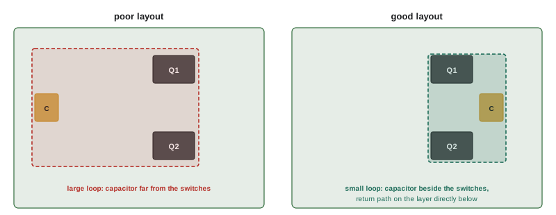
- Minimize the area of high-\(di/dt\) loops. Identify the loops in which current switches on and off (for a buck, the loop through the input capacitor, high-side switch and low-side switch) and make them as small as possible, with forward and return paths on adjacent board layers so that their magnetic fields cancel.
- Minimize the area and capacitance of high-\(dv/dt\) nodes. Keep the switching node small and away from sensitive circuits, heat sinks and enclosure walls, or shield it.
- Place decoupling capacitors close to the switches: a high-frequency ceramic capacitor right at the device, in addition to the bulk capacitors.
- Use solid ground planes, and keep power ground currents out of the signal ground used by control and sensing circuits, joining them at a single defined point.
- Route gate drive loops tightly, with the driver close to the device and its return connected to the device's source (a Kelvin source connection on the package), so that the voltage induced by the power current does not disturb the gate.
- Filter cables where they leave the enclosure, and bond the filter and cable shields to the chassis with short, wide connections.
Experienced designers sketch the critical current loops before placing any components. Problems that would be expensive to fix with filters and shielding later, after the board is made, are avoided at little cost at this stage.
Common mistakes
MistakeLeaving EMI to be fixed with filters after the design is finished.
InsteadPlan current loops, decoupling and grounding from the first layout.
MistakeTreating all conducted noise the same.
InsteadSeparate differential-mode and common-mode noise; each needs a different filter.
MistakeAdding large Y capacitors without checking leakage current.
InsteadRespect the protective earth leakage limits in safety standards.
MistakeChoosing a device rating from the DC bus voltage alone.
InsteadAdd turn-off overshoot from loop inductance and allow margin.
MistakeIgnoring snubber power loss.
InsteadEstimate C·V²·f dissipation and consider clamps, regeneration or soft switching.
Summary and key terms
- Trapezoidal switching waveforms have spectra that extend to frequencies set by the rise time.
- High dv/dt drives current through stray capacitance; high di/dt induces voltage in stray inductance.
- Differential-mode noise needs X capacitors and series inductors; common-mode noise needs chokes and Y capacitors.
- FCC Part 15 limits are close to CISPR limits; conducted emissions are measured with a LISN from 150 kHz to 30 MHz.
- An LC filter attenuates about 40 dB per decade above its corner and must be damped.
- Commutation-loop inductance causes overshoot ΔV ≈ I√(L/Coss) and high-frequency ringing.
- Snubbers, clamps, soft switching and above all tight layout control noise and overshoot.
- Electromagnetic interference (EMI)
- Unwanted electromagnetic energy that disturbs other equipment.
- Differential-mode noise
- Noise current flowing out on one conductor and back on another.
- Common-mode noise
- Noise current flowing in the same direction on all conductors and returning through ground.
- Common-mode choke
- Coupled windings that block common-mode current but pass normal current.
- Y capacitor
- A capacitor from a line to protective earth for common-mode filtering.
- LISN
- Line impedance stabilization network used to measure conducted emissions.
- Commutation loop
- The circuit path in which current transfers between devices during switching.
- Snubber
- A circuit that absorbs switching energy to limit overshoot and ringing.
- Soft switching
- Switching at zero voltage or zero current to reduce loss and noise.
- Kelvin source
- A separate source connection for the gate driver return.
Practice problems
Work each problem on paper first, then reveal the answer to check.
A switching node changes at 30 V/ns and has 20 pF to the heat sink. Common-mode current?
Show answer
20 × 10⁻¹² × 30 × 10⁹ = 0.6 A.
A current changes by 20 A in 10 ns through 15 nH. Induced voltage?
Show answer
15 × 10⁻⁹ × 2 × 10⁹ = 30 V.
How does a common-mode choke pass normal current without saturating?
Show answer
The opposing currents cancel their flux in the core.
Why are Y capacitors limited in size?
Show answer
They cause leakage current to protective earth, which safety standards limit.
What is 60 dBµV in millivolts?
Show answer
1 mV.
A filter must give 60 dB at 200 kHz. Maximum corner for one LC stage?
Show answer
200 kHz / 10^(60/40) ≈ 6.3 kHz.
Overshoot for 40 A, 8 nH and 400 pF?
Show answer
40 × √(8 × 10⁻⁹ / 4 × 10⁻¹⁰) = 40 × 4.47 ≈ 179 V.
Ringing frequency for 8 nH and 400 pF?
Show answer
1/(2π√(3.2 × 10⁻¹⁸)) ≈ 89 MHz.
Snubber loss for 1 nF at 600 V and 100 kHz?
Show answer
10⁻⁹ × 360,000 × 10⁵ = 36 W.
What is the most important layout rule for a half-bridge?
Show answer
Minimize the area of the high-di/dt commutation loop.
Lesson quiz · 5 questions
Score 60% or more to complete this lesson.
Create a free account to save your progress, take quizzes and earn a certificate.