
ELE-240 · Lesson 9 of 12 · 26 min
MOSFET biasing and switching circuits
Lesson 7 biased BJTs and used them as switches. This lesson does the same for MOSFETs. The ideas carry over directly, an operating point that must be stable against device variation, negative feedback from a source resistor, a switch that must turn fully on and fully off, but the details differ. The MOSFET's gate draws no DC current, which simplifies bias networks, while its threshold voltage varies widely between parts, which makes stable bias just as important as for a BJT. As a switch, the MOSFET's gate behaves like a capacitor that must be charged and discharged, and that is what limits switching speed and causes switching loss.
Amara's tasks are the low-side MOSFET switches that turn each signal head on and off, a pulse-width-modulation (PWM) scheme that dims the signals at night, and a biased MOSFET stage that will serve as an alternative input for the microphone amplifier, to compare with the BJT design.
DC analysis of MOSFET circuits
The procedure mirrors the BJT case. Set signal sources to zero and open the capacitors. Because the gate draws no current, the gate voltage is found directly from the gate network, often a simple divider. Assume the MOSFET is in saturation and write i_D = ½k_n'(W/L)(v_GS − V_t)² together with the equation of the source circuit. If there is a source resistor, the two equations combine into a quadratic in v_GS (or in v_OV). Of its two roots, keep the one with v_GS > V_t; the other is a mathematical artifact. Finally check v_DS ≥ v_GS − V_t; if the check fails, the device is in triode, and the triode equation must be used instead.
Why fixed gate bias is a poor choice
Setting the gate at a fixed voltage with the source grounded fixes v_GS, and the drain current then depends directly on V_t and k_n'. Discrete MOSFET datasheets typically give V_t as a range such as 1.0 to 2.5 V. With v_GS = 3 V, the overdrive could be anything from 0.5 to 2.0 V, and since current goes as the square of the overdrive, the drain current could vary sixteen to one. This is the MOSFET version of fixed base bias, and it fails for the same reason.
Voltage-divider bias with a source resistor
The cure is the same as for the BJT: a source resistor R_S that provides negative feedback. The gate is held at V_G by a divider; the source sits at I_D R_S; and v_GS = V_G − I_D R_S. If I_D tries to rise, v_GS falls and pulls it back. The larger the voltage across R_S compared with the uncertainty in V_t, the more stable the bias. Because the gate draws no current, the divider resistors can be very large, megohms, without affecting the bias, which keeps the input resistance of an amplifier high.
Worked problem
Biasing a MOSFET amplifier stage
An NMOS with k_n'(W/L) = 4 mA/V² and V_t = 1.5 V is biased from 12 V with V_G = 4 V and R_S = 2 kΩ. Find I_D and V_GS, then choose R_D for V_D = 8 V and check the region.
Show solution
- Write v_OV = V_GS − V_t and V_GS = V_G − I_D R_S, so v_OV = 2.5 − 2000 I_D.
- \[I_D = \tfrac{1}{2}(0.004)\,v_{OV}^2 = 0.002\,v_{OV}^2\]
- Substitute I_D = (2.5 − v_OV)/2000: (2.5 − v_OV)/2000 = 0.002 v_OV², so 4 v_OV² + v_OV − 2.5 = 0.
- \[v_{OV} = \frac{-1 + \sqrt{1 + 40}}{8} \approx 0.675\ \text{V}\]
- \[I_D = 0.002 \times 0.675^2 \approx 0.912\ \text{mA}, \qquad V_{GS} \approx 2.18\ \text{V}\]
- \[R_D = \frac{12 - 8}{0.912\ \text{mA}} \approx 4.4\ \text{k}\Omega \to 4.3\ \text{k}\Omega\]
- Check: V_S = 1.82 V, V_DS ≈ 8.1 − 1.82 = 6.3 V ≥ v_OV = 0.68 V, so the MOSFET is in saturation.
Answer: I_D ≈ 0.91 mA with V_GS ≈ 2.18 V. The negative root of the quadratic would give v_OV < 0, which is not physical, so it is discarded.
import math
# Divider bias with source degeneration: how much does I_D move as Vt varies?
VG, RS, k = 4.0, 2000.0, 4e-3           # k = kn' W/L
def bias(Vt):
    # (VG - Vt - ID*RS) = vov ; ID = k/2 vov^2  ->  (k*RS/2) vov^2 + vov - (VG - Vt) = 0
    a, b, c = k * RS / 2, 1.0, -(VG - Vt)
    vov = (-b + math.sqrt(b * b - 4 * a * c)) / (2 * a)
    return k / 2 * vov**2, vov
for Vt in (1.0, 1.5, 2.0, 2.5):
    ID, vov = bias(Vt)
    print(f"Vt = {Vt:.1f} V: ID = {ID*1000:.3f} mA, VGS = {Vt + vov:.2f} V")
# Compare with fixed gate bias at VGS = 3 V and RS = 0
for Vt in (1.0, 2.5):
print(f"fixed VGS = 3 V, Vt = {Vt}: ID = {k / 2 * (3 - Vt)**2 * 1000:.2f} mA")Vt = 1.0 V: ID = 1.125 mA, VGS = 1.75 V Vt = 1.5 V: ID = 0.912 mA, VGS = 2.18 V Vt = 2.0 V: ID = 0.703 mA, VGS = 2.59 V Vt = 2.5 V: ID = 0.500 mA, VGS = 3.00 V fixed VGS = 3 V, Vt = 1.0: ID = 8.00 mA fixed VGS = 3 V, Vt = 2.5: ID = 0.50 mA
Even with degeneration the current still varies over this wide threshold range, because the voltage across R_S is only about 2 V. Raising V_G and R_S together improves stability further at the cost of signal swing. In integrated circuits, where transistors on the same chip are closely matched, designers avoid the problem entirely by biasing with current mirrors.
Other bias circuits
Drain feedback bias connects a large resistor from drain to gate. Since no gate current flows, V_G = V_D, which guarantees saturation (v_DS = v_GS > v_GS − V_t) and gives negative feedback: if I_D rises, V_D falls and so does V_GS. A constant-current source in the source lead, built from another transistor, sets I_D directly and is the standard method in integrated circuits. For depletion-mode MOSFETs and JFETs, which conduct with zero gate voltage, a simple self-bias with only a source resistor and a grounded gate resistor works, because the voltage across R_S makes v_GS negative.
The MOSFET as a low-side switch
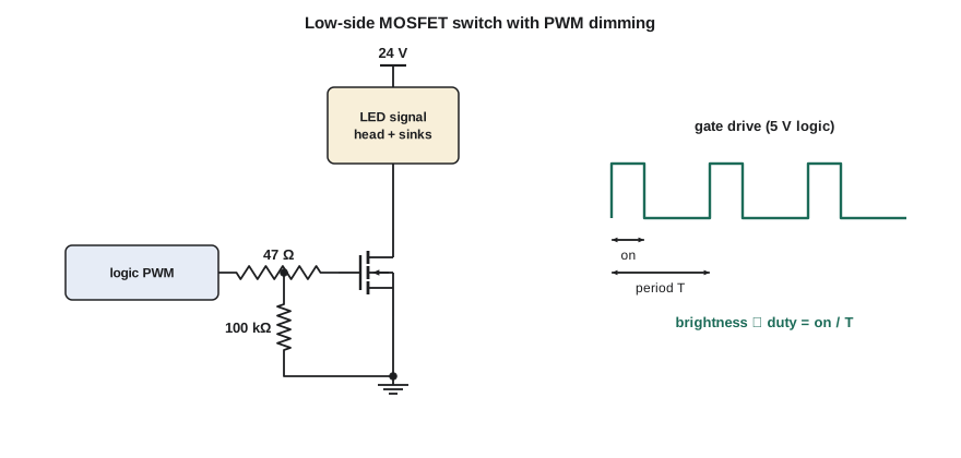
A MOSFET switch is as simple as it gets: load from the supply to the drain, source to ground, and a logic signal on the gate. When the gate is high, the MOSFET is in the triode region with only R_DS(on) between drain and source; when the gate is low, it is cut off. There is no base current to supply, so a single logic pin can switch amps. Two things must be checked: that R_DS(on) is specified at the actual gate drive voltage, and that the conduction loss, I²R_DS(on), is within the package's thermal capability.
Worked problem
Switching a signal head
Each signal head draws up to 1.2 A from 24 V. The candidate logic-level MOSFET has R_DS(on) = 45 mΩ at V_GS = 4.5 V (typical 25 °C) and 70 mΩ maximum at 4.5 V and 125 °C, and its package has θ_JA = 60 °C/W on Cedarline's board. The logic output is 5 V. Find the worst-case conduction loss and junction temperature at a 74 °C cabinet ambient.
Show solution
- \[P = I^2 R_{DS(on),max} = 1.2^2 \times 0.070 \approx 0.10\ \text{W}\]
- \[T_J = T_A + P\,\theta_{JA} = 74 + 0.10 \times 60 \approx 80\ ^\circ\text{C}\]
Answer: The MOSFET dissipates only about 0.1 W and runs near 80 °C, comfortably below its 150 °C limit. A BJT switch at the same current would drop about 0.2 to 0.3 V and need tens of milliamps of base current.
Gate charge and switching speed
The gate of a MOSFET is a capacitor, and to turn the device on, the driver must deliver its total gate charge Q_g, typically a few nanocoulombs for a small part and up to a few hundred for a large one. During switching, the gate voltage rises to threshold, then pauses on the Miller plateau while the drain voltage swings and the gate–drain capacitance is charged, then rises to its final value. The switching time is roughly the charge needed divided by the gate current, which is the drive voltage minus the plateau voltage, divided by the gate resistance:
While the MOSFET switches, both voltage and current are present at once, so it dissipates power during each transition. The switching loss is roughly ½V_DS I_D (t_r + t_f) f_sw. At low frequencies it is negligible; at the hundreds of kilohertz used in switch-mode power supplies, it can dominate, which is why power-supply MOSFETs are chosen for low gate charge and driven by dedicated gate-driver chips that source and sink amps. The gate resistor is a compromise: smaller means faster switching and less switching loss, larger means slower edges and less electromagnetic interference and ringing.
# Conduction and switching loss of the signal-head MOSFET under PWM dimming
VDS, ID, Rds = 24.0, 1.2, 0.070
Qgd, RG, Vdrive, Vplat = 3e-9, 47.0, 5.0, 2.6
tsw = Qgd * RG / (Vdrive - Vplat)            # one edge
for fpwm, duty in ((1000, 1.0), (1000, 0.3), (20000, 0.3)):
    p_cond = ID**2 * Rds * duty
    p_sw = 0.5 * VDS * ID * (2 * tsw) * fpwm
    print(f"f = {fpwm:6d} Hz, duty {duty:.0%}: conduction {p_cond*1000:6.1f} mW, switching {p_sw*1000:7.3f} mW")
print(f"edge time about {tsw*1e9:.0f} ns")f = 1000 Hz, duty 100%: conduction 100.8 mW, switching 1.692 mW f = 1000 Hz, duty 30%: conduction 30.2 mW, switching 1.692 mW f = 20000 Hz, duty 30%: conduction 30.2 mW, switching 33.840 mW edge time about 59 ns
PWM dimming
To dim the signals at night, the controller switches each signal head on and off rapidly with pulse-width modulation. The eye averages the light, so the apparent brightness is proportional to the duty cycle, the fraction of each period the switch is on. The frequency must be high enough to avoid visible flicker, which for LEDs viewed by moving observers means at least a few hundred hertz, and preferably above about 1 kHz to avoid the stroboscopic effect seen when the eyes move. Low frequencies keep switching losses tiny and electromagnetic interference low; Cedarline uses 1 kHz. Because the LED current sinks from lesson 7 hold the current constant whenever the head is on, PWM changes brightness without changing color, which is not the case when LEDs are dimmed by reducing their current.
Inductive loads and high-side switches
Switching an inductive load such as a relay, solenoid or motor needs a flyback diode just as for a BJT, or the drain voltage will spike at turn-off. Power MOSFETs are rated for some avalanche energy, so they can survive small inductive kicks without a diode, but relying on that is poor practice for repetitive switching. Sometimes the load must be switched on its supply side, so that it is grounded when off; this needs a high-side switch. A PMOS is the simplest choice: its source goes to the supply, and pulling its gate down below the source by more than its threshold turns it on. Because a 3.3 V logic output cannot pull the gate of a 24 V PMOS all the way up to 24 V to turn it off, a small NPN or NMOS level shifter drives the PMOS gate, with a resistor holding it at the source voltage when off and a Zener clamping v_GS to protect the gate. High-current high-side switches often use an NMOS instead, with a bootstrap or charge-pump gate driver that lifts its gate above the supply rail.
Worked problem
Level-shifted PMOS high-side switch
A PMOS with V_t = −2 V and V_GS(max) = ±20 V switches a 24 V heater. An NMOS level shifter pulls the PMOS gate down through 10 kΩ, with 10 kΩ from gate to source. What is V_SG when on, and is the gate safe?
Show solution
- When the level shifter is on, the two 10 kΩ resistors divide the 24 V:
- \[V_{SG} = 24 \times \frac{10}{10 + 10} = 12\ \text{V}\]
- 12 V is well above |V_t| = 2 V and below the 20 V gate rating.
Answer: The PMOS sees V_SG = 12 V when on, which turns it fully on while keeping the gate oxide safe. With the level shifter off, V_SG = 0 and the PMOS is off.
Common mistakes
MistakeKeeping the wrong root of the bias quadratic.
InsteadChoose the root with v_GS > V_t; the other gives a negative overdrive.
MistakeUsing fixed gate bias with a discrete MOSFET.
InsteadV_t spreads widely between parts; add source degeneration or use a current source.
MistakeAssuming a MOSFET switches instantly because its gate draws no DC current.
InsteadThe gate charge must be supplied; speed depends on gate current and Q_g.
MistakeDriving a high-side PMOS gate directly from low-voltage logic.
InsteadUse a level shifter so the gate can reach the source voltage, and clamp v_GS within its rating.
Summary and key terms
- MOSFET DC analysis: find V_G from the divider, assume saturation, solve the quadratic and check v_DS ≥ v_OV.
- Fixed gate bias is unstable because V_t varies widely; a source resistor gives negative feedback.
- Drain feedback and current-source bias are other stable options.
- A MOSFET switch needs R_DS(on) specified at the actual gate drive and acceptable I²R loss.
- Switching speed and switching loss depend on gate charge and gate drive current.
- PWM dims LEDs by duty cycle; high-side switching uses a PMOS with a level shifter or an NMOS with a boosted gate drive.
- Source degeneration
- Negative feedback from a resistor in the source lead that stabilizes the operating point.
- Drain feedback bias
- A bias circuit with a resistor from drain to gate, which guarantees saturation.
- Gate charge
- The total charge Q_g needed to switch a MOSFET's gate from off to fully on.
- Miller plateau
- The flat part of the gate-voltage waveform while the gate–drain capacitance charges during switching.
- Switching loss
- Energy dissipated while voltage and current overlap during each transition.
- PWM
- Pulse-width modulation, controlling average power by the fraction of time a switch is on.
- High-side switch
- A switch placed between the supply and the load, so the load is grounded when off.
Practice problems
Work each problem on paper first, then reveal the answer to check.
V_G = 3 V, R_S = 1 kΩ, k_n'(W/L) = 2 mA/V², V_t = 1 V. Find I_D.
Show answer
(2 − v_OV)/1000 = 0.001 v_OV² → v_OV² + v_OV − 2 = 0 → v_OV = 1 V, I_D = 1 mA.
With fixed v_GS = 2.5 V, how much does I_D change as V_t goes from 1 V to 2 V (same k)?
Show answer
It scales as (1.5)² : (0.5)² = 9 : 1.
A MOSFET carries 3 A with R_DS(on) = 25 mΩ. Find the conduction loss.
Show answer
3² × 0.025 = 0.225 W.
Q_gd = 5 nC, R_G = 10 Ω, V_drive = 10 V, V_plateau = 4 V. Estimate the switching time.
Show answer
5 nC × 10 / 6 V ≈ 8.3 ns.
What duty cycle gives 25 % of full brightness with PWM?
Show answer
25 %.
Why does drain feedback bias guarantee saturation?
Show answer
With V_D = V_G, v_DS = v_GS, which is always greater than v_GS − V_t.
Lesson quiz · 5 questions
Score 60% or more to complete this lesson.
Create a free account to save your progress, take quizzes and earn a certificate.