
ELE-240 · Lesson 1 of 12 · 25 min
Semiconductors and the pn junction
Every transistor, diode, light-emitting diode, solar cell and integrated circuit is built from a semiconductor, a material whose ability to carry current lies between that of a metal and that of an insulator and, more importantly, can be controlled. Electronics I is the course where circuit analysis meets these devices. In ELE-202 you treated resistors, capacitors, sources and op amps as ideal elements with simple equations. Here you learn what is inside the parts that make amplifiers, power supplies, switches and logic gates possible, how to model them well enough to design with them, and where the simple models stop being true.
In an ABET-accredited American electrical or computer engineering program, Electronics I normally comes in the spring of the sophomore year, after circuit analysis and alongside signals and digital logic. It leads to Electronics II (ELE-340), which covers differential amplifiers, feedback, oscillators and output stages, and to power electronics. The skills you build here, reading a datasheet, choosing a bias point and checking a design against worst-case conditions, are exactly the ones an engineer intern is asked to show on a first hardware job.
The examples continue at Cedarline Controls, the invented Madison, Wisconsin company from ELE-210 that designs controllers for traffic signals and small machines. Amara Osei, an engineer intern, and Daniel Fortin, the senior hardware designer, are now working on the analog side of the pedestrian crossing controller: the power supply that turns the cabinet's AC feed into clean DC rails, the drivers for the walk and don't-walk LED signal heads, the input circuit for the shaft-speed sensor on the tachometer, and a small microphone amplifier for the accessible pedestrian signal, which raises its locator tone when the street gets noisy. Every lesson takes one piece of that hardware.
Conductors, insulators and semiconductors
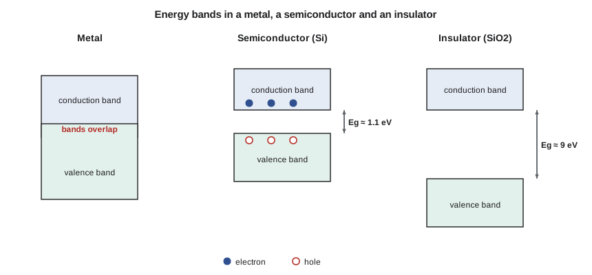
In a solid, the electrons of neighboring atoms interact so strongly that their allowed energies spread into bands. The highest band that is completely filled at absolute zero is the valence band; the next band up is the conduction band. Between them lies a range of energies that electrons cannot have, the band gap, written E_g and measured in electron-volts (eV). Current can flow only if electrons can move into nearby empty states, so a full band carries no current and an empty band has no carriers. What matters is how easily electrons can reach the conduction band.
In a metal the bands overlap, so there are always free electrons and the material conducts well at any temperature. In an insulator such as glass or silicon dioxide the band gap is large, about 9 eV for SiO₂, and almost no electrons gain enough energy to cross it. A semiconductor has a modest gap: 1.12 eV for silicon, about 1.4 eV for gallium arsenide and about 3.3 eV for silicon carbide. At room temperature a small fraction of electrons is thermally excited across the gap, so a pure semiconductor conducts a little, and that conductivity rises steeply with temperature, the opposite of a metal.
Electrons and holes
Silicon has four valence electrons, and in a crystal each atom shares one electron with each of its four neighbors in covalent bonds. When heat breaks a bond, a free electron moves into the conduction band and leaves behind a vacancy in the valence band. A neighboring bound electron can hop into that vacancy, which moves the vacancy the other way. It is far easier to track the vacancy than the many electrons shuffling around it, so we treat it as a particle in its own right: a hole, with charge +q, where q = 1.602 × 10⁻¹⁹ C is the magnitude of the electron charge.
In pure, or intrinsic, silicon, electrons and holes are created in pairs, so their concentrations are equal. Each is written n_i, the intrinsic carrier concentration. At 300 K, n_i for silicon is about 1.0 × 10¹⁰ cm⁻³. That sounds large, but silicon has about 5 × 10²² atoms per cubic centimeter, so only one atom in roughly five trillion contributes a carrier. The intrinsic concentration depends strongly on temperature,
where B is a material constant, T is the absolute temperature and k = 8.617 × 10⁻⁵ eV/K is Boltzmann's constant. For silicon near room temperature, n_i roughly doubles for every 11 °C rise. This single fact explains why diode leakage current doubles about every 10 °C and why every transistor bias design must be checked hot as well as cold.
Doping: n-type and p-type silicon
Pure silicon is not useful for devices. What makes semiconductors so valuable is that their carrier concentrations can be set precisely by adding tiny amounts of impurities, a process called doping. If a few silicon atoms are replaced by phosphorus or arsenic, which have five valence electrons, four of the five form bonds and the fifth is so loosely held that at room temperature it is free. These atoms are donors, and silicon doped with them is n-type: electrons are the majority carriers and holes the minority carriers. If boron, with three valence electrons, is added instead, each boron atom leaves a missing bond that captures an electron from the valence band and creates a hole. Boron is an acceptor, and the result is p-type silicon, with holes as the majority carriers.
Typical doping concentrations run from about 10¹⁵ to 10¹⁹ atoms per cubic centimeter, still only a few parts per million or less, but far larger than n_i. In n-type silicon with donor concentration N_D, the electron concentration is essentially n ≈ N_D. The hole concentration then follows from the mass-action law, which holds in thermal equilibrium for doped or undoped material:
Doping one type of carrier up pushes the other down. This is why minority carriers, few as they are, matter so much in diodes and bipolar transistors: the device currents are set by how many minority carriers can be injected across a junction.
Worked problem
Carrier concentrations in a sensor-input diode
The protection diode on the tachometer input is made from n-type silicon doped with N_D = 10¹⁶ cm⁻³ of phosphorus. Find the electron and hole concentrations at 300 K, taking n_i = 1.0 × 10¹⁰ cm⁻³.
Show solution
- All donors are ionized at room temperature, so the electron concentration equals the donor concentration.
- \[n \approx N_D = 1.0 \times 10^{16}\ \text{cm}^{-3}\]
- Use the mass-action law for the minority holes.
- \[p = \frac{n_i^2}{n} = \frac{(1.0 \times 10^{10})^2}{1.0 \times 10^{16}} = 1.0 \times 10^{4}\ \text{cm}^{-3}\]
- The ratio of majority to minority carriers is 10¹², a trillion to one.
Answer: n ≈ 1.0 × 10¹⁶ cm⁻³ and p ≈ 1.0 × 10⁴ cm⁻³. The doping raised the electron concentration a million-fold and cut the hole concentration a million-fold.
Drift and diffusion
Carriers move for two reasons. Drift is motion caused by an electric field: electrons move against the field and holes with it, at an average velocity proportional to the field, v = μE, where μ is the mobility. In lightly doped silicon at room temperature, electron mobility is about 1,350 cm²/V·s and hole mobility about 480 cm²/V·s. Electrons are almost three times as mobile, which is why n-channel MOSFETs and npn transistors are faster and stronger than their p-type partners of the same size. Drift current density in a material with both carriers is
so the conductivity σ, and its inverse the resistivity ρ, depend directly on doping. This is how integrated-circuit resistors are made: a strip of doped silicon whose resistance is set by its doping, length and width.
Diffusion is motion caused by a difference in concentration. Carriers move randomly, and where there are more of them on one side than the other, more wander from the crowded side to the sparse side than back again, giving a net flow. The diffusion current is proportional to the concentration gradient, with a diffusion constant D. Mobility and diffusion constant are linked by the Einstein relation, D/μ = kT/q. The quantity kT/q, the thermal voltage V_T, is about 25.9 mV at 300 K and appears in nearly every equation in this course.
The pn junction at equilibrium
A pn junction is formed when p-type and n-type regions meet in a single crystal. It is the heart of the diode and, doubled, of the bipolar transistor. At the moment the regions meet, the n side has many electrons and the p side many holes, so electrons diffuse into the p side and holes into the n side. Each carrier that crosses recombines with a majority carrier of the other type, and it leaves behind an ionized dopant atom that is fixed in the crystal: positive donor ions on the n side, negative acceptor ions on the p side.
This thin layer of uncovered fixed charge on either side of the junction is the depletion region, so called because it has almost no free carriers. Its charge creates an electric field pointing from the n side to the p side, and that field pushes carriers back the way they came, opposing diffusion. Equilibrium is reached when the drift caused by the field exactly balances diffusion. The potential difference across the depletion region at equilibrium is the built-in voltage,
which for typical silicon doping is between about 0.6 and 0.9 V. The built-in voltage cannot be measured with a voltmeter, because contact potentials at the metal terminals cancel it exactly, but it sets the forward voltage at which a diode starts to conduct strongly.
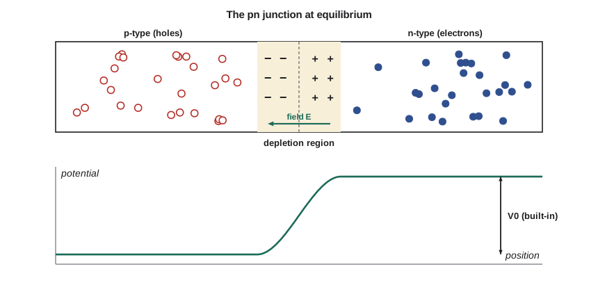
The width of the depletion region depends on the doping. Charge on the two sides must balance, so the region extends further into the more lightly doped side. For a junction with N_A much larger than N_D, almost all of the depletion width lies on the n side. Typical widths are a fraction of a micrometer at zero bias.
Here ε_s ≈ 1.04 × 10⁻¹² F/cm is the permittivity of silicon and V_R is any reverse voltage applied. The width grows with the square root of the total voltage across the junction.
Forward and reverse bias
Applying a voltage changes the barrier. With the p side made positive relative to the n side, forward bias, the applied voltage opposes the built-in field. The barrier drops, the depletion region narrows, and diffusion wins: holes pour into the n side and electrons into the p side, where they become minority carriers and recombine. The number that can climb the reduced barrier grows exponentially with the forward voltage, which gives the diode its exponential current. With the n side made positive, reverse bias, the barrier rises, the depletion region widens, and diffusion stops. Only a tiny current of minority carriers generated thermally near the junction flows, the reverse saturation current I_S, typically 10⁻¹⁵ to 10⁻¹² A in a small silicon diode at room temperature.
The result is the Shockley diode equation, the most important single equation in electronics:
The ideality factor n is between 1 and 2; it is close to 1 for the base-emitter junction of a transistor and closer to 2 for some power diodes. Lesson 2 builds the practical models designers use from this equation.
import math
q, k = 1.602e-19, 1.381e-23          # C, J/K
T = 300.0
VT = k * T / q
ni = 1.0e10                          # silicon, cm^-3 at 300 K
NA, ND = 1e17, 1e16                  # p side and n side doping, cm^-3
eps = 11.7 * 8.854e-14               # silicon permittivity, F/cm

V0 = VT * math.log(NA * ND / ni**2)
print(f"thermal voltage VT = {VT*1000:.2f} mV")
print(f"built-in voltage V0 = {V0:.3f} V")
for VR in (0.0, 5.0, 12.0):
    W = math.sqrt(2 * eps / q * (1/NA + 1/ND) * (V0 + VR))
    xn = W * NA / (NA + ND)          # part of the width on the n side
print(f"VR = {VR:4.1f} V: W = {W*1e4:.3f} um, n-side share {xn/W:.0%}")thermal voltage VT = 25.86 mV built-in voltage V0 = 0.774 V VR = 0.0 V: W = 0.332 um, n-side share 91% VR = 5.0 V: W = 0.906 um, n-side share 91% VR = 12.0 V: W = 1.348 um, n-side share 91%
The output shows two facts designers lean on. The built-in voltage is a little under 0.8 V for this doping, and the depletion region widens as reverse voltage rises. A wider depletion region also means less capacitance, which lesson 5 uses for varactor diodes.
Junction capacitance and breakdown
A reverse-biased junction stores charge in its depletion region, so it behaves like a capacitor whose plates are the edges of the region. Because the width changes with voltage, so does the capacitance: C_j = C_j0 / (1 + V_R/V_0)^m, with m between about 0.33 and 0.5. Forward-biased junctions also store minority charge in the neutral regions, the diffusion capacitance, which grows with current. These two capacitances limit how fast diodes and transistors switch and set the upper frequency limit of amplifiers in lesson 12.
If the reverse voltage is made large enough, the junction breaks down and conducts heavily. In heavily doped junctions the depletion region is so thin that electrons tunnel straight through it, Zener breakdown, below about 5 V. In more lightly doped junctions, carriers accelerated by the strong field knock electrons out of bonds, which are themselves accelerated, an avalanche. Breakdown is not damaging in itself as long as the power stays within limits, and lesson 4 shows how Zener diodes use it to hold a voltage steady.
| Quantity | Symbol | Typical silicon value at 300 K |
|---|---|---|
| Band gap | E_g | 1.12 eV |
| Intrinsic concentration | n_i | ≈ 1.0 × 10¹⁰ cm⁻³ |
| Electron mobility (light doping) | μ_n | ≈ 1,350 cm²/V·s |
| Hole mobility (light doping) | μ_p | ≈ 480 cm²/V·s |
| Thermal voltage | V_T | ≈ 25.9 mV |
| Built-in voltage | V₀ | 0.6 to 0.9 V |
| Reverse saturation current (small diode) | I_S | 10⁻¹⁵ to 10⁻¹² A |
From physics to circuit models
Device physics can go much deeper, into band bending, recombination rates and quantum effects, but a circuit designer needs only enough to understand what the models mean and when they fail. Daniel Fortin puts it this way to new engineers at Cedarline: know why the diode current is exponential, know why it doubles with temperature, know where the capacitance comes from, and then trust a good model and verify on the bench. The rest of this course follows that path. Lesson 2 turns the junction into practical diode models, and lessons 6 and 8 do the same for the two kinds of transistor.
Common mistakes
MistakeThinking holes are just missing atoms or positive ions.
InsteadA hole is a missing electron in a covalent bond that moves through the crystal; fixed ions in the depletion region are a different thing and cannot move.
MistakeAssuming doping makes a semiconductor electrically charged.
InsteadEach donor or acceptor brings its own balancing charge, so doped silicon is neutral; only the depletion region carries net charge.
MistakeUsing the built-in voltage as something you can measure with a meter.
InsteadContact potentials cancel it; it shows up indirectly as the forward voltage where conduction becomes large.
MistakeForgetting temperature.
Insteadn_i, I_S and leakage all rise steeply with temperature; I_S roughly doubles every 5 °C and leakage about every 10 °C.
Summary and key terms
- Semiconductors have a band gap small enough that heat, light and doping control their carrier concentration.
- Current is carried by electrons in the conduction band and holes in the valence band.
- Donors make n-type material and acceptors make p-type; the mass-action law np = n_i² links the two carrier concentrations.
- Carriers move by drift in a field and by diffusion down a concentration gradient; V_T = kT/q ≈ 25.9 mV links the two.
- A pn junction forms a depletion region and a built-in voltage that balance diffusion and drift.
- Forward bias lowers the barrier and gives an exponential current; reverse bias leaves only a tiny saturation current until breakdown.
- Band gap
- The range of forbidden energies between the valence and conduction bands; 1.12 eV for silicon.
- Hole
- A vacancy in the valence band that behaves as a mobile positive carrier.
- Donor
- An impurity with five valence electrons, such as phosphorus, that gives n-type silicon.
- Acceptor
- An impurity with three valence electrons, such as boron, that gives p-type silicon.
- Depletion region
- The layer at a pn junction that has lost its free carriers and holds fixed ionized dopants.
- Built-in voltage
- The potential across the depletion region at equilibrium, V₀ = V_T ln(N_A N_D / n_i²).
- Thermal voltage
- V_T = kT/q, about 25.9 mV at 300 K.
Practice problems
Work each problem on paper first, then reveal the answer to check.
Silicon is doped with 5 × 10¹⁷ cm⁻³ of boron. Find the hole and electron concentrations at 300 K.
Show answer
p ≈ 5 × 10¹⁷ cm⁻³; n = n_i²/p = 10²⁰ / 5 × 10¹⁷ = 200 cm⁻³.
Why are npn transistors usually faster than pnp transistors of the same size?
Show answer
Their main current is carried by electrons, whose mobility is about three times that of holes.
Find V₀ for N_A = N_D = 10¹⁶ cm⁻³ at 300 K.
Show answer
V₀ = 0.0259 ln(10³² / 10²⁰) = 0.0259 × ln(10¹²) ≈ 0.716 V.
In a junction with N_A = 10¹⁸ cm⁻³ and N_D = 10¹⁵ cm⁻³, which side holds most of the depletion region?
Show answer
The lightly doped n side; the widths are inversely proportional to the doping, so about 99.9 % is on the n side.
Reverse leakage of a diode is 10 nA at 25 °C. Estimate it at 85 °C.
Show answer
Doubling every 10 °C gives 2⁶ = 64 times larger, about 640 nA.
Does the depletion width increase or decrease with reverse bias, and what happens to the junction capacitance?
Show answer
The width increases with the square root of the total voltage, so the capacitance decreases.
Lesson quiz · 5 questions
Score 60% or more to complete this lesson.
Create a free account to save your progress, take quizzes and earn a certificate.