
ELE-240 · Lesson 8 of 12 · 21 min
MOSFETs: physics and characteristics
The metal-oxide-semiconductor field-effect transistor, or MOSFET, is the most manufactured device in history. A modern processor holds tens of billions of them, and the same basic device, scaled up, switches hundreds of amps in electric vehicle inverters and power supplies. Unlike the BJT, the MOSFET is controlled by a voltage on an insulated gate that draws essentially no DC current. That single property makes it ideal for logic, where millions of gates must each draw almost no power at rest, and for power switching, where a small gate driver can control a very large load. This lesson explains how the MOSFET works and develops the equations used to design with it.
At Cedarline, MOSFETs appear in three places: logic-level power MOSFETs that switch the 24 V supply to each signal head, a P-channel MOSFET that replaces the lossy series diode for reverse-polarity protection, and the CMOS logic and microcontroller that run the whole controller, whose gates are MOSFETs too.
Structure
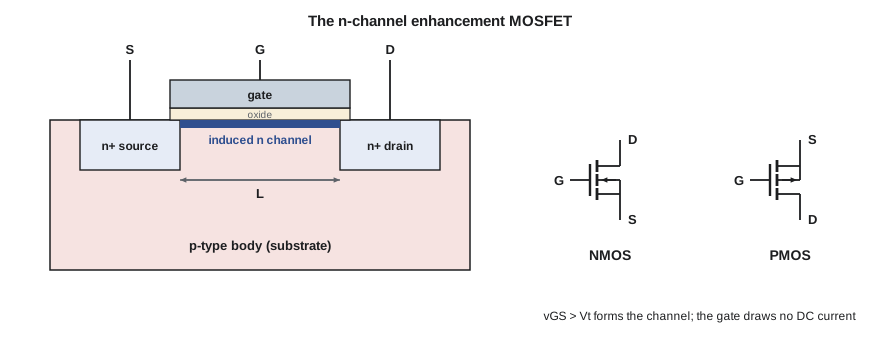
An n-channel enhancement MOSFET, or NMOS transistor, starts with a lightly doped p-type substrate, also called the body. Two heavily doped n⁺ regions, the source and the drain, are formed in it a short distance apart; that distance is the channel length L, and the width of the regions is the channel width W. Over the gap between them sits a very thin insulating layer, originally silicon dioxide, a few nanometers thick in modern logic and tens of nanometers in discrete parts, and on top of that a conducting gate electrode. The gate, the oxide and the silicon form a capacitor, and that capacitor is the key to the device.
Threshold and the induced channel
With the gate at the same voltage as the source and body, the source and drain are two back-to-back pn junctions with the p-type body between them, and no current flows. Making the gate positive pushes holes away from the surface under the gate, leaving a depletion layer, and then attracts electrons. When the gate voltage reaches the threshold voltage V_t, enough electrons gather at the surface to make a thin n-type layer, an inversion layer, connecting source and drain. This is the channel. Above threshold, every extra volt on the gate adds more electrons to the channel in proportion to the oxide capacitance per unit area, C_ox = ε_ox / t_ox. The amount by which v_GS exceeds threshold is the overdrive voltage, v_OV = v_GS − V_t, and the channel charge is proportional to it.
Threshold voltages range from about 0.3 to 0.5 V in modern logic processes to 1 to 4 V in discrete power MOSFETs. Logic-level power MOSFETs are designed with V_t around 1 to 2 V and are specified with their on-resistance at a gate voltage of 4.5 V or even 2.5 V, so they can be driven straight from a logic output. Standard power MOSFETs need about 10 V on the gate to turn fully on.
Triode region
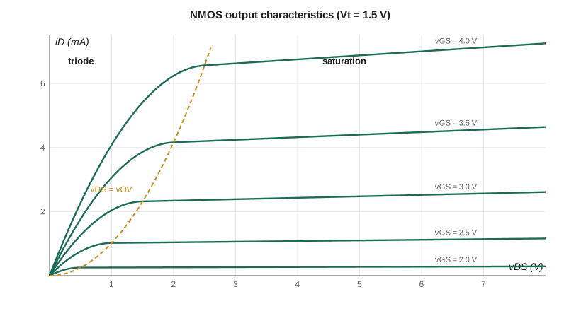
With a channel present and a small drain-to-source voltage, the channel acts as a resistor: current flows from drain to source in proportion to v_DS, and the resistance falls as the overdrive rises. As v_DS increases, the channel near the drain becomes shallower, because the gate-to-channel voltage there is v_GS − v_DS, smaller than at the source end. Accounting for this taper gives the triode-region equation, valid for v_DS < v_OV:
Here k_n' = μ_n C_ox is the process transconductance parameter, set by the manufacturing process, and W/L is the aspect ratio, which the designer chooses. For very small v_DS the squared term is negligible and the MOSFET is a voltage-controlled resistor, r_DS = 1/[k_n'(W/L)v_OV]. Power MOSFETs used as switches run in this region, and their datasheets give the result directly as R_DS(on), the on-resistance at a stated gate voltage, often a few milliohms to a few ohms.
Saturation region
When v_DS reaches v_OV, the channel depth at the drain end falls to zero; the channel is said to be pinched off. Increasing v_DS further hardly changes the current, because the extra voltage appears across a short depleted region near the drain, which sweeps arriving electrons across. The current saturates at the value reached at pinch-off:
This square-law relation is the MOSFET's counterpart to the BJT's exponential law. Saturation here means the opposite of BJT saturation: a MOSFET in saturation is the one acting as an amplifier or current source, with the current set by v_GS and nearly independent of v_DS, just like a BJT in its active mode. The terms are confusing, but they are universal, so it pays to memorize the match: MOSFET saturation corresponds to BJT active, and MOSFET triode corresponds roughly to BJT saturation.
| Region | Condition (NMOS) | Drain current | Use |
|---|---|---|---|
| Cutoff | v_GS < V_t | i_D ≈ 0 | Switch off |
| Triode | v_GS > V_t and v_DS < v_GS − V_t | k_n'(W/L)[v_OV v_DS − v_DS²/2] | Switch on, voltage-controlled resistor |
| Saturation | v_GS > V_t and v_DS ≥ v_GS − V_t | ½k_n'(W/L)v_OV²(1 + λv_DS) | Amplifier, current source |
Channel-length modulation and the body effect
In saturation the current rises slightly with v_DS, because the pinched-off region grows and the effective channel gets shorter, just as the Early effect thins a BJT's base. The effect is modeled by a factor (1 + λv_DS), where λ is typically 0.01 to 0.1 V⁻¹ and larger for short channels. It gives an output resistance r_o = 1/(λI_D) = V_A/I_D, with V_A = 1/λ. A second effect matters in integrated circuits: if the source is above the body, the threshold rises, the body effect, because a larger depletion charge must be overcome. In discrete MOSFETs the source and body are connected internally, so the body effect does not appear.
Worked problem
Operating region and current
An NMOS transistor has V_t = 1.5 V and k_n'(W/L) = 2 mA/V², with λ = 0. Find the region and drain current for v_GS = 3 V with v_DS = 5 V, and with v_DS = 0.5 V.
Show solution
- \[v_{OV} = 3 - 1.5 = 1.5\ \text{V}\]
- With v_DS = 5 V ≥ 1.5 V the device is in saturation:
- \[i_D = \tfrac{1}{2}(2)(1.5)^2 = 2.25\ \text{mA}\]
- With v_DS = 0.5 V < 1.5 V it is in the triode region:
- \[i_D = 2\big[(1.5)(0.5) - \tfrac{1}{2}(0.5)^2\big] = 2(0.75 - 0.125) = 1.25\ \text{mA}\]
Answer: 2.25 mA in saturation; 1.25 mA in triode. At the boundary v_DS = 1.5 V the two equations give the same current, 2.25 mA, as they must.
# NMOS output characteristics from the square-law model with channel-length modulation
Vt, k, lam = 1.5, 2.0e-3, 0.02          # V, A/V^2 (k = kn' W/L), 1/V
def i_d(vgs, vds):
    vov = vgs - Vt
    if vov <= 0:
        return 0.0, "cutoff"
    if vds < vov:
        return k * (vov * vds - vds**2 / 2) * (1 + lam * vds), "triode"
    return 0.5 * k * vov**2 * (1 + lam * vds), "saturation"

for vgs in (2.0, 3.0, 4.0):
    pts = []
    for vds in (0.25, 0.5, 1.0, 2.0, 5.0, 10.0):
        i, region = i_d(vgs, vds)
        pts.append(f"{i*1000:6.2f}{region[0]}")
    print(f"vGS = {vgs} V: " + "  ".join(pts))
print("(t = triode, s = saturation)")
vov = 1.5
print(f"on-resistance near vDS = 0 at vGS = 3 V: {1 / (k * vov):.0f} ohm")
print(f"output resistance at 2.25 mA: {1 / (lam * 2.25e-3) / 1000:.0f} kOhm")vGS = 2.0 V: 0.19t 0.25s 0.26s 0.26s 0.28s 0.30s vGS = 3.0 V: 0.69t 1.26t 2.04t 2.34s 2.48s 2.70s vGS = 4.0 V: 1.19t 2.27t 4.08t 6.24t 6.88s 7.50s (t = triode, s = saturation) on-resistance near vDS = 0 at vGS = 3 V: 333 ohm output resistance at 2.25 mA: 22 kOhm
P-channel MOSFETs and CMOS
A p-channel MOSFET, or PMOS, is built in an n-type body with p⁺ source and drain, and conducts by holes. Everything is reversed: it turns on when the gate is more negative than the source by more than |V_t|, its current flows from source to drain, and its equations use v_SG, v_SD and |V_t|. Because holes are slower, a PMOS needs about two to three times the width of an NMOS for the same current. Combining an NMOS and a PMOS gives a CMOS inverter, the basis of all modern digital logic, as ELE-210 described: one transistor is always off in either logic state, so the gate draws almost no current except while switching.
PMOS transistors are also the natural high-side switch. Amara's reverse-polarity protection uses one with its drain on the input connector and its source toward the board, with the gate pulled to ground. With the supply connected correctly, current first flows through the MOSFET's internal body diode, raising the source; the gate is then far below the source, the channel turns on and bypasses the diode, and the voltage drop falls from about 0.7 V to I × R_DS(on), perhaps 15 mV at 180 mA with an 80 mΩ part. Reversed, the body diode blocks and the gate-to-source voltage is zero, so the MOSFET stays off. A Zener between gate and source protects the thin gate oxide from the full 24 V.
Power MOSFETs
Discrete power MOSFETs use a vertical structure, with the source on top, the drain on the bottom of the die and thousands of small cells in parallel, giving very low on-resistance. Every power MOSFET contains a body diode from source to drain (for NMOS), which conducts if the drain is pulled below the source; this is a nuisance in some circuits and an advantage in others, such as motor drives where it acts as a free flyback diode. Key datasheet figures are V_DS(max), I_D, R_DS(on) at a stated gate voltage and temperature (it roughly doubles from 25 °C to 150 °C), the gate threshold range, the total gate charge Q_g, which sets how hard the gate must be driven to switch quickly, and the maximum gate-source voltage, typically ±20 V. Exceeding the gate voltage rating punctures the oxide and destroys the device.
Comparing MOSFETs and BJTs
MOSFETs draw no DC gate current, have no minority-carrier storage, so they switch fast and cleanly, and their positive temperature coefficient of resistance makes paralleled devices share current naturally. BJTs, for the same current, give much higher transconductance, the ratio of output current change to input voltage change, because their law is exponential rather than square; they have more precisely predictable V_BE, which makes them better for voltage references and low-offset amplifiers; and they handle electrostatic discharge better. Lesson 10 quantifies the transconductance difference, which is why many precise analog circuits still use BJTs, while digital circuits and power switches use MOSFETs.
The square-law model is a first-order description. In modern short-channel devices, carrier velocity saturates in the strong lateral field, and the current grows closer to linearly with overdrive than with its square. Below threshold the current does not drop to zero but falls exponentially, the subthreshold region, which sets the leakage of idle logic and is used deliberately in ultra-low-power circuits. Circuit simulators use far more detailed models, but the square law is what designers use for hand analysis, and it is accurate enough for discrete devices and long-channel transistors.
Common mistakes
MistakeThinking MOSFET saturation is like BJT saturation.
InsteadMOSFET saturation is the amplifying region with current set by v_GS; MOSFET triode is the switch-on region.
MistakeForgetting to check v_DS ≥ v_OV before using the saturation equation.
InsteadAlways confirm the region; use the triode equation if v_DS < v_GS − V_t.
MistakeDriving a standard power MOSFET from 3.3 V logic.
InsteadCheck that R_DS(on) is specified at your gate voltage; choose a logic-level part.
MistakeIgnoring the body diode.
InsteadA power MOSFET conducts from source to drain through its body diode whenever the drain is pulled below the source.
Summary and key terms
- A MOSFET's gate is insulated; a gate voltage above threshold V_t induces a channel between source and drain.
- Triode: i_D = k_n'(W/L)[v_OV v_DS − v_DS²/2], a voltage-controlled resistor for small v_DS.
- Saturation (v_DS ≥ v_OV): i_D = ½k_n'(W/L)v_OV²(1 + λv_DS), used for amplification.
- Channel-length modulation gives r_o = 1/(λI_D); the body effect raises V_t when the source is above the body.
- PMOS mirrors NMOS with reversed polarities; CMOS pairs them for low-power logic.
- Power MOSFETs are specified by V_DS, R_DS(on), gate threshold and charge, and contain a body diode.
- Threshold voltage
- The gate-to-source voltage at which an inversion channel forms, V_t.
- Overdrive voltage
- v_OV = v_GS − V_t, the gate voltage beyond threshold.
- Triode region
- The MOSFET region with v_DS < v_OV, where the channel acts as a voltage-controlled resistor.
- Saturation region
- The MOSFET region with v_DS ≥ v_OV, where the current depends on v_GS and only weakly on v_DS.
- Aspect ratio
- W/L, the channel width divided by its length, chosen by the designer.
- R_DS(on)
- The drain–source resistance of a fully on MOSFET at a stated gate voltage.
- Body diode
- The intrinsic pn junction from source (and body) to drain in a power MOSFET.
Practice problems
Work each problem on paper first, then reveal the answer to check.
An NMOS has V_t = 0.8 V and k_n'(W/L) = 4 mA/V². Find i_D at v_GS = 1.8 V in saturation.
Show answer
½ × 4 × 1² = 2 mA.
For the same device, what v_GS gives 8 mA in saturation?
Show answer
v_OV = √(2 × 8/4) = 2 V, so v_GS = 2.8 V.
Find r_DS near v_DS = 0 for v_GS = 2.8 V.
Show answer
1/(4 mA/V² × 2 V) = 125 Ω.
v_GS = 2 V, V_t = 1 V, v_DS = 0.6 V. Which region?
Show answer
Triode, because v_DS = 0.6 V < v_OV = 1 V.
Find r_o for λ = 0.05 V⁻¹ at I_D = 1 mA.
Show answer
1/(0.05 × 0.001) = 20 kΩ.
A power MOSFET has R_DS(on) = 20 mΩ at 25 °C. Estimate its conduction loss at 10 A with the junction near 125 °C.
Show answer
R_DS(on) roughly 1.7 to 2 times higher, about 36 mΩ; P ≈ 10² × 0.036 ≈ 3.6 W.
Lesson quiz · 5 questions
Score 60% or more to complete this lesson.
Create a free account to save your progress, take quizzes and earn a certificate.