
ELE-240 · Lesson 6 of 12 · 24 min
Bipolar junction transistors: physics and characteristics
The bipolar junction transistor, or BJT, was the device that made modern electronics possible. Invented at Bell Laboratories in the late 1940s, it replaced vacuum tubes in radios, computers and hearing aids, and although MOSFETs now dominate integrated circuits, BJTs remain everywhere in discrete and analog design: in precise amplifiers, current sources, voltage references, radio-frequency circuits, LED and relay drivers and power-supply controllers. A BJT is two pn junctions back to back, sharing a very thin middle layer, and its essential trick is that a small current into that middle layer controls a much larger current through the device.
Amara's LED current sink from lesson 5 needs a transistor, and so do the relay drivers that switch the cabinet's flash transfer relays and the input stage of the microphone amplifier. Daniel standardizes on a general-purpose small-signal npn transistor in the 2N3904 class for low-current work: rated about 40 V and 200 mA, with a current gain of roughly 100 to 300.
Structure and symbols
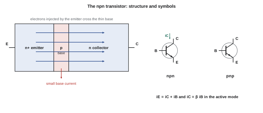
An npn transistor has an n-type emitter, a thin p-type base and an n-type collector. The emitter is very heavily doped, the base is lightly doped and extremely thin, often well under a micrometer in a modern device, and the collector is moderately doped and large. A pnp transistor reverses all three. The circuit symbol has an arrow on the emitter showing the direction of conventional current through the base–emitter junction when it is forward biased: out of the emitter for npn (Not Pointing iN), into the emitter for pnp.
How the transistor works
In normal amplifier use, the active mode, the base–emitter junction is forward biased and the base–collector junction is reverse biased. The forward-biased emitter junction injects a flood of electrons from the heavily doped emitter into the base. Because the base is thin and lightly doped, very few of these electrons find a hole to recombine with before they diffuse to the edge of the collector junction. There, the strong field of the reverse-biased junction sweeps them into the collector. The collector current is therefore set by how many electrons the emitter injects, which depends exponentially on v_BE, exactly as in a diode:
The base current has two small parts: holes injected from the base back into the emitter, which is small because the emitter is so much more heavily doped, and holes needed to replace those lost to recombination in the base. Both are proportional to the collector current, so their ratio is fixed. This ratio is the common-emitter current gain β, also written h_FE on datasheets:
With β = 100, the base current is 1 percent of the collector current and α = 0.99: 99 percent of the electrons leaving the emitter reach the collector. That is the source of current gain. It is important to see what controls what. Physically, v_BE controls i_C exponentially, and the base current is a by-product. In circuit design it is often convenient to think of the base current controlling the collector current through β, but β is a poorly controlled parameter, and good designs never depend on its exact value.
Worked problem
Currents in an active transistor
A transistor with β = 150 has I_S = 2 × 10⁻¹⁵ A and is biased with v_BE = 0.65 V at 25 °C (V_T = 25.7 mV). Find i_C, i_B, i_E and α.
Show solution
- \[i_C = I_S e^{v_{BE}/V_T} = 2 \times 10^{-15}\, e^{0.65/0.0257} \approx 0.193\ \text{mA}\]
- \[i_B = \frac{i_C}{\beta} = \frac{0.193}{150} \approx 1.29\ \mu\text{A}\]
- \[i_E = i_C + i_B \approx 0.194\ \text{mA}, \qquad \alpha = \frac{150}{151} \approx 0.993\]
Answer: About 0.19 mA flows in the collector, controlled by a base current of only 1.3 µA. Raising v_BE by V_T ln 2 ≈ 18 mV would double i_C, and each 60 mV multiplies it by about ten.
The four operating modes
Each junction can be forward or reverse biased, which gives four modes. Analog amplifiers use the active mode. Digital and switching circuits use cutoff, where both junctions are reverse biased and the transistor is off, and saturation, where both are forward biased and the transistor acts as a closed switch with a small voltage V_CE(sat) of about 0.1 to 0.3 V. The reverse active mode, with the roles of emitter and collector swapped, works but with very low gain and is rarely used deliberately.
| Mode | Base–emitter junction | Base–collector junction | Behavior | Typical use |
|---|---|---|---|---|
| Cutoff | Reverse (or below ~0.5 V) | Reverse | Off; only leakage flows | Switch open |
| Active | Forward (≈ 0.7 V) | Reverse | i_C = βi_B, set by v_BE | Amplifiers, current sources |
| Saturation | Forward | Forward | v_CE ≈ 0.2 V; i_C < βi_B | Switch closed |
| Reverse active | Reverse | Forward | Very low gain | Rare; some logic circuits |
A quick test for an npn transistor in a circuit: if v_BE is about 0.7 V and v_CE is more than about 0.3 V, it is active; if v_CE is down near 0.2 V, it is saturated; if v_BE is well below 0.5 V, it is cut off.
Characteristic curves
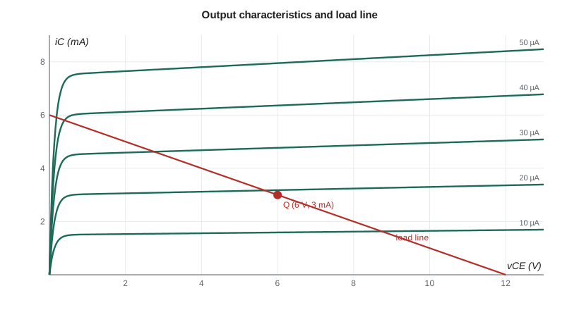
The input characteristic, i_B against v_BE, is simply a diode curve: almost nothing below 0.5 V and a steep rise near 0.6 to 0.7 V. Like any junction, v_BE falls about 2 mV per °C at constant current. The output characteristics plot i_C against v_CE for several fixed base currents. Each curve rises steeply from the origin through the saturation region, bends sharply at about v_CE = 0.2 to 0.3 V, and then runs almost flat across the active region, where the collector current depends on the base current and hardly at all on v_CE.
The Early effect
The active-region curves are not perfectly flat; they slope gently upward. As v_CE rises, the collector junction's depletion region widens and eats into the base, so the effective base gets thinner, fewer electrons are lost, and i_C rises a little. This is the Early effect, after James Early who explained it. Extended backward, the curves all meet the voltage axis near a single point, −V_A, where V_A is the Early voltage, typically 50 to 150 V for small-signal transistors. The effect is modeled by
The output resistance r_o is the inverse slope of the curve. At I_C = 1 mA and V_A = 100 V, r_o = 100 kΩ. It is large but not infinite, and it limits the gain of amplifiers in lesson 11 and the quality of current sources.
Current gain is not a constant
Datasheets give β as a range, often three to one or wider between units of the same type: a 2N3904-class part might list h_FE from 100 to 300 at 10 mA. β also rises with temperature, roughly 0.5 to 1 percent per °C, and varies with collector current, falling at very low currents and again at high currents. A design that works only for one value of β will not survive production. Lesson 7 shows bias circuits whose operating point depends very little on β, which is the central idea of good BJT design.
import math
VT, Is, VA = 0.0257, 2e-15, 100.0
# Output characteristics: iC versus vCE for several base currents (beta = 150)
beta = 150
print(" vCE(V) " + "".join(f"  iB={ib:2d}uA" for ib in (10, 20, 30, 40)))
for vce in (0.5, 2, 4, 6, 8, 10, 12):
    row = []
    for ib in (10, 20, 30, 40):
        ic = beta * ib * 1e-6 * (1 + vce / VA)   # active region with Early effect
        row.append(f"{ic*1000:9.3f}mA")
    print(f"{vce:7.1f} " + " ".join(row))
# Small-signal output resistance at 1 mA
print(f"ro at IC = 1 mA: {VA / 1e-3 / 1000:.0f} kOhm")
# vBE needed for 1 mA, and its temperature drift (about -2 mV per degree C)
vbe = VT * math.log(1e-3 / Is)
print(f"vBE at 1 mA, 25 C: {vbe:.3f} V; at 75 C about {vbe - 0.002 * 50:.3f} V") vCE(V) iB=10uA iB=20uA iB=30uA iB=40uA
0.5 1.507mA 3.015mA 4.522mA 6.030mA
2.0 1.530mA 3.060mA 4.590mA 6.120mA
4.0 1.560mA 3.120mA 4.680mA 6.240mA
6.0 1.590mA 3.180mA 4.770mA 6.360mA
8.0 1.620mA 3.240mA 4.860mA 6.480mA
10.0 1.650mA 3.300mA 4.950mA 6.600mA
12.0 1.680mA 3.360mA 5.040mA 6.720mA
ro at IC = 1 mA: 100 kOhm
vBE at 1 mA, 25 C: 0.692 V; at 75 C about 0.592 VThe load line and the Q-point
A transistor in a circuit must also obey the external circuit. For the common arrangement with a collector resistor R_C from a supply V_CC, Kirchhoff's voltage law gives v_CE = V_CC − i_C R_C, a straight line on the output characteristics running from (V_CC, 0) to (0, V_CC/R_C). The transistor's operating point lies on this load line, at the intersection with the curve for the actual base current. For an amplifier, the Q-point is placed near the middle of the line's active section, so the collector voltage can swing both up and down. For a switch, the transistor is driven between cutoff at one end of the line and saturation at the other.
Worked problem
Q-point on the load line
With V_CC = 12 V and R_C = 2 kΩ, a transistor with β = 150 has a base current of 20 µA. Ignoring the Early effect, find the Q-point, and the base current that would just saturate the transistor (take V_CE(sat) = 0.2 V).
Show solution
- \[I_C = \beta I_B = 150 \times 20\ \mu\text{A} = 3.0\ \text{mA}\]
- \[V_{CE} = 12 - 3.0\ \text{mA} \times 2\ \text{k}\Omega = 6.0\ \text{V}\]
- At the edge of saturation the collector current is limited by the resistor:
- \[I_{C,sat} = \frac{12 - 0.2}{2000} = 5.9\ \text{mA} \quad\Rightarrow\quad I_{B,edge} = \frac{5.9}{150} \approx 39\ \mu\text{A}\]
Answer: The Q-point is (6.0 V, 3.0 mA), the middle of the load line, ideal for an amplifier. Any base current above about 39 µA saturates the transistor.
Limits and ratings
Every transistor has a safe operating area bounded by maximum collector current, maximum collector–emitter voltage V_CEO (with the base open), maximum power dissipation and, for power transistors, a second-breakdown limit at high voltage and current together. Power dissipation in the active mode is P = V_CE I_C + V_BE I_B ≈ V_CE I_C, and it heats the junction above ambient by P times the thermal resistance θ_JA, often about 200 °C/W for a small plastic package with no heatsink. A 2N3904-class part in free air can therefore dissipate only about 0.6 W at 25 °C ambient, and less in a hot cabinet. Because β and leakage rise with temperature, a transistor that heats up conducts more and heats further; without a bias design that resists it, this thermal runaway can destroy the part.
The pnp transistor
A pnp transistor works the same way with every polarity reversed: the emitter injects holes, the base is n-type, currents flow out of the base and collector and into the emitter, and in active mode the emitter is the most positive terminal, with v_EB ≈ 0.7 V. Holes are slower than electrons, so pnp transistors are somewhat slower and weaker than npn of the same size, but they are indispensable as high-side switches, in current mirrors and in complementary push-pull output stages. Daniel's flash relay driver, for example, uses a pnp to switch the 24 V side of the relay coil.
Common mistakes
MistakeThinking the base current physically causes the collector current.
Insteadv_BE controls i_C exponentially; i_B is a small by-product with ratio β.
MistakeDesigning for one exact value of β.
Insteadβ varies three to one or more between parts and with temperature; good designs work over the whole range.
MistakeCalling a transistor active when v_CE is 0.2 V.
InsteadThat is saturation; i_C is then set by the external circuit and is less than βi_B.
MistakeIgnoring dissipation in small packages.
InsteadP ≈ V_CE I_C heats the junction by P × θ_JA; a small plastic transistor manages well under a watt.
Summary and key terms
- A BJT is two junctions sharing a thin, lightly doped base between a heavily doped emitter and a collector.
- In active mode, i_C = I_S e^{v_BE/V_T}, i_B = i_C/β and i_E = (β + 1) i_B.
- Cutoff and saturation make the transistor a switch; active mode makes it an amplifier.
- Output characteristics are nearly flat in the active region; the slope is the Early effect, r_o = V_A/I_C.
- β varies widely with part, temperature and current, so designs must not depend on its exact value.
- Check current, voltage, power and thermal limits; pnp transistors mirror npn with polarities reversed.
- BJT
- A bipolar junction transistor, in which both electrons and holes take part in conduction.
- Current gain β
- The ratio of collector current to base current in the active mode, also written h_FE.
- Active mode
- Base–emitter forward biased and base–collector reverse biased; used for amplification.
- Saturation
- Both junctions forward biased; the transistor acts as a closed switch with small V_CE.
- Early effect
- The rise of i_C with v_CE caused by base-width modulation, modeled by the Early voltage V_A.
- Output resistance
- r_o = V_A / I_C, the inverse slope of the output characteristic.
- Thermal runaway
- Self-reinforcing heating in which rising temperature increases current, which raises temperature further.
Practice problems
Work each problem on paper first, then reveal the answer to check.
A transistor has i_C = 4 mA and i_B = 25 µA. Find β, α and i_E.
Show answer
β = 160, α = 160/161 ≈ 0.994, i_E = 4.025 mA.
How much must v_BE change to multiply i_C by 10 at room temperature?
Show answer
V_T ln 10 ≈ 59 mV, about 60 mV.
Find r_o at I_C = 0.5 mA with V_A = 80 V.
Show answer
80 / 0.5 mA = 160 kΩ.
An npn has V_BE = 0.68 V and V_CE = 0.15 V. Which mode is it in?
Show answer
Saturation, because both junctions are forward biased (V_BC = 0.53 V).
With V_CC = 9 V and R_C = 1.5 kΩ, where does the load line meet the axes?
Show answer
At V_CE = 9 V and I_C = 9/1.5 kΩ = 6 mA.
A small transistor has θ_JA = 200 °C/W and a 150 °C maximum junction temperature. What can it dissipate at 70 °C ambient?
Show answer
(150 − 70)/200 = 0.4 W.
Lesson quiz · 5 questions
Score 60% or more to complete this lesson.
Create a free account to save your progress, take quizzes and earn a certificate.