
CMP-240 · Lesson 7 of 12 · 25 min
Op-amps and comparators as building blocks
The operational amplifier, or op-amp, is the most useful analog building block a digital designer meets. With two or three resistors it becomes a buffer that isolates a soft source from its load, an amplifier that scales a tiny sensor voltage up to fill the ADC's range, or a circuit that subtracts one voltage from another. Its close relative, the comparator, turns an analog voltage into a clean logic signal. You do not need to know the transistor circuit inside an op-amp to use one well; a simple model and two rules are enough for most designs, and the circuit analysis methods from lessons 4 to 6 do the rest.
The NS-4 uses three op-amp circuits. A buffer drives the ADC from the battery divider, an amplifier measures the solar charging current from the 50 mΩ sense resistor, and a comparator watches the battery voltage and cuts power to the radar if the battery runs too low, protecting it from deep discharge. Jonah is asked to check all three for the NS-5.
The op-amp model
An op-amp has two inputs, the non-inverting input (+) and the inverting input (−), one output and two supply pins. It amplifies the difference between its inputs by a very large open-loop gain A, typically 100,000 or more at low frequencies. A useful circuit model is a voltage-controlled voltage source: the output equals A times (v₊ − v₋), drawn behind a small output resistance, with a very large input resistance between the inputs. The output can never go beyond the supply rails; a rail-to-rail output op-amp gets within a few tens of millivolts of each rail, and older designs stay a volt or more away.
Because A is so large, an op-amp used on its own saturates at one rail or the other for almost any input difference: with A = 100,000, a difference of just 33 µV drives the output across a 3.3 V range. Op-amps become useful when negative feedback connects part of the output back to the inverting input. The feedback adjusts the output until the inputs are almost equal, and the circuit's behavior is then set by the external resistors rather than by the poorly controlled value of A.
The two golden rules
For an ideal op-amp with negative feedback and an output that is not saturated, two rules give the answer to almost every circuit. First, no current flows into either input, because the input resistance is effectively infinite. Second, the output does whatever is needed to make the voltage difference between the inputs zero, so v₋ = v₊. The second rule is sometimes called the virtual short: the inputs sit at the same voltage, but no current flows between them. Apply the rules with KCL at the inverting input and almost any op-amp circuit can be solved in a few lines.
The voltage follower
The simplest feedback circuit connects the output directly to the inverting input and the signal to the non-inverting input. By the second rule the output equals the input. The circuit has a gain of exactly one, so it seems to do nothing, but it has an input resistance of many megohms and an output resistance of a fraction of an ohm. It copies a voltage from a soft source to a load without loading the source, which is why it is called a buffer.
Worked problem
Buffering the battery divider
Lesson 6 found that the battery divider is a 2.72 V source behind 21.3 kΩ, too soft to charge the ADC's sampling capacitor quickly. Ines considers a follower between the divider and the ADC. The op-amp's input bias current is 1 nA and its output resistance with feedback is 0.1 Ω. Find the error caused by the bias current and the follower's effective source resistance seen by the ADC.
Show solution
- The bias current flows through R_Th, causing a drop:
- \[\Delta v = I_B R_{Th} = 1\ \text{nA} \times 21.3\ \text{k}\Omega = 21\ \mu\text{V}\]
- One step of a 12-bit, 3.3 V ADC is 3.3/4096 = 0.81 mV, so 21 µV is negligible.
- The ADC now sees the follower's output resistance, about 0.1 Ω instead of 21.3 kΩ, so the sampling capacitor charges in nanoseconds.
Answer: The follower removes the sampling problem completely and adds an error smaller than one fortieth of an ADC step. It costs an op-amp, about 1 µA to 50 µA of supply current depending on the part, and board space. Ines decides the reservoir capacitor from lesson 6 is good enough for the battery reading, but keeps the follower for the thermistor, whose network has a higher resistance.
Non-inverting and inverting amplifiers
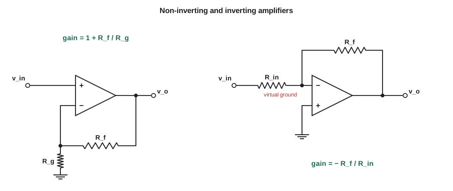
Adding a resistive divider in the feedback path gives gain. In the non-inverting amplifier, the signal drives the + input and a divider of R_f and R_g feeds a fraction of the output back to the − input. The output settles where that fraction equals the input, so the gain is one plus the resistor ratio. The input resistance is still very high.
In the inverting amplifier, the + input is grounded and the signal drives the − input through R_in, with R_f from output to − input. By the second rule the − input sits at 0 V, a virtual ground, so the input current is v_in/R_in. By the first rule that current cannot enter the op-amp, so it all flows through R_f, making the output −R_f/R_in times the input. The inverting amplifier's input resistance is only R_in, but its virtual ground makes it ideal for summing several signals, each through its own resistor.
The difference amplifier and current sensing
The NS-4 charger's 50 mΩ sense resistor drops only 75 mV at 1.5 A, and one end of it sits at the battery voltage rather than at ground. A difference amplifier measures the voltage across the resistor while rejecting the common voltage that both ends share. With four resistors matched in the ratio R₂/R₁, its output is (R₂/R₁)(v₂ − v₁). Choosing R₂/R₁ = 20 turns 75 mV into 1.5 V. In practice, high-side current measurement is usually done with a dedicated current-sense amplifier, a difference amplifier with precision-matched resistors built in, because ordinary 1 percent resistors limit how well the common voltage is rejected.
Worked problem
Scaling the charging current
The charge current flows through the 50 mΩ resistor and the ADC reads 0 to 3.3 V. Choose the amplifier's gain so that the largest expected current, 1.8 A including a margin above the charger's 1.5 A limit, gives about 3.0 V. Find the ADC voltage and the current resolution of a 12-bit conversion.
Show solution
- \[v_{sense,max} = 1.8 \times 0.050 = 90\ \text{mV}\]
- \[G = \frac{3.0}{0.090} = 33.3 \;\Rightarrow\; \text{choose } G = 33 \ (R_1 = 3.0\ \text{k}\Omega,\ R_2 = 100\ \text{k}\Omega \text{ gives } 33.3)\]
- \[v_{ADC}(1.5\ \text{A}) = 1.5 \times 0.05 \times 33.3 = 2.50\ \text{V}\]
- \[\Delta I = \frac{3.3/4096}{0.05 \times 33.3} = \frac{0.806\ \text{mV}}{1.667\ \Omega} = 0.48\ \text{mA per step}\]
Answer: A gain of about 33 puts the charger's full 1.5 A at 2.5 V with headroom to 1.8 A, and each ADC step represents about half a milliampere, ample for measuring how much charge the battery receives in a day.
Comparators
A comparator compares two voltages and outputs a logic level: high if v₊ > v₋ and low otherwise. It is designed to be used without negative feedback, to switch quickly between rails, and often to have an open-drain output that can drive a logic input or an LED directly. You can use an op-amp as a comparator in a pinch, but a true comparator switches faster, recovers from saturation cleanly and is specified for this job.
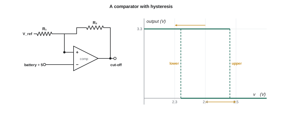
A plain comparator has a problem with slowly changing or noisy inputs. As the battery voltage drifts down past the threshold, small noise from the radar's current pulses makes it cross back and forth, and the output chatters on and off many times. If that output switches a load, the load's own current changes the battery voltage and makes the chatter worse. The cure is hysteresis: positive feedback from the output to the + input, through a resistor, so that the threshold moves away from the input once the output switches. The circuit is called a Schmitt trigger, and it has two thresholds, a rising one and a falling one.
Worked problem
The low-battery cutoff
The cutoff must switch the radar off when the battery falls to 11.6 V and back on only when it recovers to 12.4 V. A divider of ratio 0.2 feeds the battery voltage to the comparator's − input, so the thresholds at the comparator are 2.32 V and 2.48 V. The + input connects to a reference V_ref through R₁ and to the output through R₂. The output swings from 0 to 3.3 V, and high means cut off the radar. Choose R₂/R₁ and V_ref.
Show solution
- Let k = R₁/(R₁ + R₂), the fraction of the output fed back. By superposition, v₊ = V_ref(1 − k) + v_o k.
- With the battery healthy the output is low, so v₊ = V_ref(1 − k). When the falling battery takes v₋ below this, the output goes high: this is the lower threshold, 2.32 V.
- With the output high, v₊ = V_ref(1 − k) + 3.3k. The recovering battery must lift v₋ above this before the output returns low: this is the upper threshold, 2.48 V.
- \[V_{T,high} - V_{T,low} = 3.3k = 0.16\ \text{V} \;\Rightarrow\; k = 0.0485, \quad \frac{R_2}{R_1} = \frac{1 - k}{k} = 19.6\]
- Choose R₁ = 10 kΩ and R₂ = 200 kΩ, giving k = 1/21 = 0.0476 and a band of 0.157 V.
- \[V_{ref} = \frac{V_{T,low}}{1 - k} = \frac{2.32}{0.9524} = 2.436\ \text{V} \approx 2.44\ \text{V}\]
Answer: A ratio R₂/R₁ of 20 gives a hysteresis band of about 0.16 V at the comparator, or 0.8 V at the battery, and a reference of about 2.44 V places the band so the radar cuts off near 11.6 V and returns near 12.4 V. Noise smaller than 0.8 V at the battery can no longer make the output chatter.
The derivation above shows a common design pattern: the width of a Schmitt trigger's hysteresis band depends only on the resistor ratio and the output swing, and its center depends on the reference. Choose the ratio for the width first, then adjust the reference to put the band in the right place. The code below checks the final values.
# Low-battery Schmitt trigger: thresholds from the resistor ratio and reference
def thresholds(v_ref, r1, r2, v_out_high=3.3, v_out_low=0.0):
    k = r1 / (r1 + r2)                       # fraction of the output fed back
    t_hi = v_ref * (1 - k) + v_out_high * k  # threshold while output is high
    t_lo = v_ref * (1 - k) + v_out_low * k   # threshold while output is low
    return t_lo, t_hi

ratio = 0.2                                  # battery divider ratio
for v_ref in (2.50, 2.44):
    lo, hi = thresholds(v_ref, 10e3, 200e3)
    print("Vref %.2f V: comparator thresholds %.3f / %.3f V -> battery %.2f / %.2f V"
          % (v_ref, lo, hi, lo / ratio, hi / ratio))

# Finite open-loop gain: how close is a non-inverting amplifier to its ideal gain?
def closed_loop(A, Rf, Rg):
    beta = Rg / (Rf + Rg)
    return A / (1 + A * beta)

for A in (1e3, 1e5, 1e6):
    g = closed_loop(A, 100e3, 3e3)
print("A = %8.0f: gain %.3f (ideal %.3f), error %.3f%%" % (A, g, 1 + 100 / 3, (1 - g / (1 + 100 / 3)) * 100))Vref 2.50 V: comparator thresholds 2.381 / 2.538 V -> battery 11.90 / 12.69 V Vref 2.44 V: comparator thresholds 2.324 / 2.481 V -> battery 11.62 / 12.40 V A = 1000: gain 33.194 (ideal 34.333), error 3.319% A = 100000: gain 34.322 (ideal 34.333), error 0.034% A = 1000000: gain 34.332 (ideal 34.333), error 0.003%
Finite gain and the limits of the ideal model
The golden rules assume infinite gain. With finite gain A and feedback fraction β = R_g/(R_f + R_g), the non-inverting amplifier's gain is A/(1 + Aβ). When Aβ is large this approaches 1/β, the ideal gain, with a fractional error of about 1/(Aβ). The code shows that A = 100,000 gives a gain error of 0.03 percent for a gain of 33, far smaller than the 1 percent resistors that set the gain. Real op-amps also have an input offset voltage of microvolts to millivolts, input bias currents, limited output current, a maximum rate of change of output called the slew rate, and a gain that falls with frequency, roughly in inverse proportion above a few hertz. A datasheet's gain-bandwidth product tells you how much gain is left at a given frequency, and for the slow sensor signals on the NS-4 it is never the limit.
Common mistakes
MistakeApplying the virtual-short rule to a comparator or a saturated op-amp.
InsteadThe rule holds only with negative feedback and an output inside its range.
MistakeAssuming the output can reach the supply rails.
InsteadCheck the output swing; only rail-to-rail parts get close to the rails.
MistakeUsing a plain comparator on a slow or noisy input.
InsteadAdd hysteresis with positive feedback so the output cannot chatter.
MistakeForgetting that the inverting amplifier's input resistance is only R_in.
InsteadUse a non-inverting stage or a buffer when the source is soft.
MistakeExpecting a difference amplifier to reject common voltage with ordinary resistors.
InsteadRejection depends on resistor matching; use a dedicated current-sense amplifier for high-side measurement.
Summary and key terms
- An op-amp amplifies v₊ − v₋ by a very large gain; with negative feedback the external resistors set the circuit's behavior.
- Golden rules: no current into the inputs, and v₋ = v₊ when feedback is negative and the output is not saturated.
- The follower buffers a soft source; non-inverting gain is 1 + R_f/R_g and inverting gain is −R_f/R_in.
- A difference amplifier measures a voltage across a resistor while rejecting a common voltage.
- Comparators turn analog levels into logic; hysteresis (a Schmitt trigger) prevents chatter on noisy or slow inputs.
- Op-amp
- A high-gain differential amplifier used with external feedback components.
- Negative feedback
- Feeding part of the output back to oppose the input, which stabilizes gain.
- Virtual short
- The condition v₋ ≈ v₊ in an op-amp with negative feedback.
- Voltage follower
- An op-amp connected for unity gain, used as a buffer.
- Comparator
- A circuit that outputs a logic level showing which of two inputs is larger.
- Hysteresis
- A difference between the rising and falling switching thresholds that prevents chatter.
- Rail-to-rail
- An op-amp whose output (or input) range extends close to both supply rails.
Practice problems
Work each problem on paper first, then reveal the answer to check.
A non-inverting amplifier has R_f = 47 kΩ and R_g = 10 kΩ. What is its gain?
Show answer
1 + 4.7 = 5.7.
An inverting amplifier with R_in = 10 kΩ and R_f = 30 kΩ receives 0.5 V. What is the output?
Show answer
−1.5 V.
Why does an op-amp with no feedback act as a comparator?
Show answer
Its huge gain drives the output to a rail for any appreciable input difference.
A Schmitt trigger has a 0.2 V hysteresis band. Will 50 mV of noise make it chatter?
Show answer
No, the noise is smaller than the band.
What does a voltage follower do for a 50 kΩ source driving a 5 kΩ load?
Show answer
It presents a very high input resistance to the source and drives the 5 kΩ load from a near-zero output resistance, so the source is not pulled down.
Lesson quiz · 5 questions
Score 60% or more to complete this lesson.
Create a free account to save your progress, take quizzes and earn a certificate.