
ELE-360 · Lesson 11 of 12 · 26 min
Waveguides and printed-circuit interconnects
A coaxial cable guides a wave between two conductors. A hollow metal pipe can guide a wave too, with no centre conductor at all, provided the frequency is high enough; and a printed-circuit trace guides a wave between itself and the ground plane beneath it, partly in the board and partly in the air. This lesson looks at guided waves in these structures. Hollow waveguides are rare in a product like the TLR-1, but their physics explains two things that matter a great deal to it: why a ventilation hole in an enclosure can block radio waves, and why a metal box can resonate. Printed-circuit transmission lines are everywhere in the product, and designing them, and the return paths under them, is a large part of making a radio work and of keeping a digital board quiet.
Modes: TEM, TE and TM
A guided wave travels along the structure, say in z, with a field pattern across it that repeats. The pattern is called a mode. In a two-conductor line filled with one uniform dielectric, the dominant mode has both E and H entirely transverse to z: a transverse electromagnetic or TEM mode. TEM modes propagate at any frequency down to DC, and their Z₀, voltage and current are well defined, which is why the transmission-line theory of lessons 9 and 10 applies. A hollow pipe, with only one conductor, cannot support a TEM mode, because there is nowhere for the electric field lines to end between conductors. Its modes have a component of H along z (transverse electric, TE) or of E along z (transverse magnetic, TM), and each mode propagates only above its own cut-off frequency.
The rectangular waveguide
In a rectangular metal pipe of inner width a and height b, with a > b, the fields must satisfy the wave equation inside and the conductor boundary condition, zero tangential E, on the walls. The solutions are standing-wave patterns across the guide, with m half-wavelengths across the width and n across the height, combined with a travelling wave along it. Each TE_mn or TM_mn mode has a cut-off frequency at which its transverse standing wave just fits. The dominant mode is TE₁₀, one half-wavelength across the width and uniform across the height, with cut-off frequency c/(2a) in an air-filled guide. Between the TE₁₀ cut-off and the next mode's cut-off, only TE₁₀ propagates, and waveguides are used in that range.
Above cut-off, the guide wavelength λ_g is longer than the free-space wavelength, and the phase velocity is faster than light, while the group velocity, which carries energy and information, is slower: the product of the two equals c². The wave can be pictured as two plane waves zigzagging between the side walls at an angle that becomes steeper as the frequency falls toward cut-off; at cut-off they bounce straight across and make no progress. The wave impedance of a TE mode, the ratio of transverse E to transverse H, is larger than η₀ and rises toward infinity at cut-off.
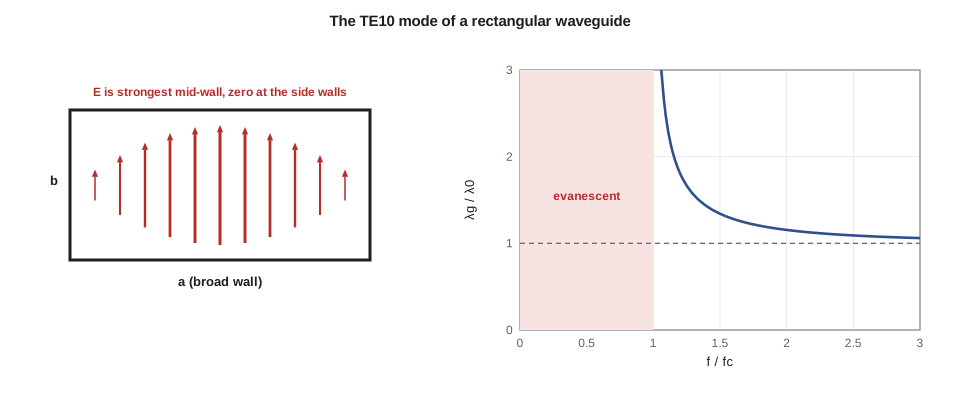
Waveguides are bulky at 915 MHz; the standard size for the band, WR-975, is 247.65 mm wide, with a TE₁₀ cut-off near 605 MHz. They are used in high-power broadcast and industrial heating systems, and at microwave and millimetre-wave frequencies, where they are small and have much lower loss than coaxial cable. For an engineer working on a 915 MHz radio, the important consequence of waveguide theory is the opposite case: what happens below cut-off.
Below cut-off: evanescent fields and ventilation holes
Below its cut-off frequency, a mode does not propagate; its fields decay exponentially along the guide. The attenuation constant is α = (2π/λ_c)√(1 − (f/f_c)²), and well below cut-off it is nearly 2π/λ_c, independent of frequency. A circular hole of radius r is a circular waveguide whose lowest mode, TE₁₁, has cut-off wavelength λ_c = 2πr/1.841. A 6 mm hole has a cut-off near 29 GHz, so at 915 MHz it is far below cut-off, and fields decay by about 27 dB for every centimetre of depth through it. A short tube, or a thick panel with holes, therefore acts as a waveguide-below-cut-off vent: air passes freely while radio waves are strongly attenuated. Honeycomb vents on shielded rooms and enclosures use this principle. A hole in a thin sheet does not get the benefit, because there is no length of guide, and the slot rule of lesson 8 applies instead.
There is a catch. A conductor passing through the hole, such as a wire or a screw, turns the hole into a coaxial line, which has a TEM mode with no cut-off. Energy then passes through freely along the conductor. That is why cables entering a shielded enclosure must have their shields bonded to the enclosure all round at the entry point, with a gland or a filtered connector, rather than simply passing through a hole: an unfiltered wire carries interference straight through any shield.
Cavity resonances
Close both ends of a waveguide and you have a cavity, a metal box that resonates at frequencies where standing waves fit in all three dimensions. The resonant frequencies of a rectangular box of dimensions a × b × d are f = (c/2)√((m/a)² + (n/b)² + (p/d)²) for suitable mode indices, at least two of which must be non-zero. Cavities with high-conductivity walls have very high Q and are used as filters and as the frequency-determining elements of microwave oscillators. In an electronic enclosure, cavity resonance is a nuisance: at a resonance, a small amount of energy leaking from a circuit builds up to large fields that couple into every other circuit in the box.
The TLR-1 enclosure is 160 × 60 × 120 mm. Its lowest resonance comes out near 1.56 GHz, and the next few lie between 2.2 and 2.8 GHz. The radio's own 915 MHz signal is below all of them, which is good; its second harmonic at 1.83 GHz and third at 2.75 GHz are not, and the third lies close to a cluster of resonances. Amara keeps the radio module inside its own small shield can, whose resonances are far higher, and adds a sheet of thin microwave absorber to the inside of the lid to lower the Q of the box resonances. The same reasoning explains why a fully populated cabinet with a 2.4 GHz Wi-Fi radio can show unexpected interference that disappears when the door is opened: opening the door destroys the cavity.
Printed-circuit transmission lines
On a printed-circuit board, a trace over a ground plane forms a microstrip line. Its fields lie partly in the dielectric beneath the trace and partly in the air above, so the mode is not quite TEM, but at the frequencies of interest it behaves like one, a quasi-TEM mode, with an effective permittivity ε_eff between 1 and ε_r. A trace buried between two ground planes is a stripline, a true TEM line entirely in the dielectric. A trace with ground on both sides in the same layer, and usually a plane below as well, is a grounded coplanar waveguide, popular in compact radio layouts because its impedance depends mainly on the gaps beside the trace and because closely spaced ground vias along its edges suppress unwanted modes.
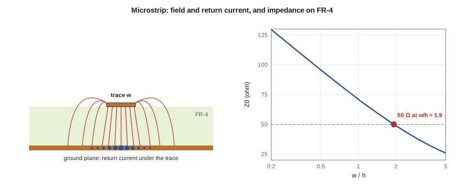
These closed-form fits, due to Hammerstad and others, are accurate to a percent or two for thin traces and are what most online calculators implement; field solvers and the board fabricator's own stack-up calculations give the final values, including copper thickness, solder mask and the frequency dependence of FR-4. For FR-4 with ε_r = 4.4, a 50 Ω microstrip is about twice as wide as its height above the plane. On a two-layer board 1.6 mm thick that is a trace about 3.1 mm wide, too wide to reach the pins of a small radio chip. On a four-layer board with 0.2 mm of prepreg between the top layer and the first plane, it is about 0.38 mm wide, which is why radio boards are almost always built on multilayer stack-ups with a solid ground plane directly under the top layer.
Worked problem
The 50 Ω trace from radio chip to antenna connector
The TLR-1 board is four layers, with 0.2 mm of FR-4 (ε_r = 4.4) between the top layer and a solid ground plane. Find the width of a 50 Ω microstrip, its effective permittivity and the guide wavelength at 915 MHz, and decide whether a 25 mm trace from the radio's output filter to the connector must be treated as a transmission line.
Show solution
- Solving the fit for Z₀ = 50 Ω gives w/h ≈ 1.92, so w ≈ 0.38 mm.
- \[\varepsilon_{\text{eff}} \approx 2.7 + 1.7\,(1 + 12/1.92)^{-1/2} = 3.33\]
- \[\lambda_g = \frac{32.8\ \text{cm}}{\sqrt{3.33}} = 17.9\ \text{cm} \qquad \frac{25\ \text{mm}}{\lambda_g} = 0.14\]
Answer: A width of 0.38 mm, ε_eff of 3.33 and a guide wavelength of 17.9 cm. The 25 mm trace is about a seventh of a wavelength, so it must be a controlled 50 Ω line; if its impedance were wrong, it would transform the antenna impedance as lesson 10 described. Amara sets the trace width as a design rule in the layout tool and asks the fabricator for an impedance-controlled stack-up.
Return current and ground planes
A signal is a wave travelling between two conductors, so every signal current has a return current. At low frequencies, the return current spreads through a ground plane along the path of least resistance. At high frequencies it follows the path of least inductance, which is directly beneath the trace, concentrated in a band a few times the trace height wide. This is the field picture of lesson 7 again: the energy travels in the dielectric between the trace and the plane, and the return current is the surface current on the plane where that field ends. Anything that forces the return current away from beneath the trace enlarges the loop, increases inductance and radiation and couples the signal into neighbours.
The classic offender is a gap or split in the ground plane under a trace, perhaps to separate an analog ground from a digital ground. The return current must detour round the end of the split, the loop area balloons and the trace radiates and picks up noise as if it were a small antenna, the effect Faraday's law predicts. Changing layers through a via is another: the return current must also change planes, and if the planes are not connected by a stitching via or a capacitor nearby, the return path detours. Amara's layout rules follow directly: one continuous ground plane under every high-speed or radio trace, no traces crossing splits, a ground stitching via beside every signal via that changes layers, and rows of ground vias round the edge of the board and along radio traces at intervals well under a twentieth of a wavelength.
Crosstalk and termination
Two traces running side by side over a plane couple through their mutual capacitance and mutual inductance. A useful rule of thumb for traces over a solid plane estimates the coupling as about 1/(1 + (D/h)²), where D is the centre-to-centre spacing and h the height above the plane. Spacing traces two to three times their height above the plane reduces crosstalk to the 10 to 20 percent range or below, and since h is only 0.2 mm on the TLR-1 board, that costs little board area. Crosstalk falls rapidly with spacing because the fields of each trace are tied tightly to the plane beneath it, another benefit of thin dielectrics.
Digital signals need termination when a trace is long compared with the edge rate, as lesson 9 explained. The APS-2's codec bit clock has edges of about 2 ns and runs 8 cm across the board, longer than the critical length of about 5.5 cm for a 2 ns edge on microstrip. Its driver has an output impedance of roughly 15 Ω. A series resistor of about 33 Ω at the driver, bringing the source impedance close to the 50 Ω trace impedance, launches a half-amplitude wave that doubles at the high-impedance receiver to a full, clean edge, and the reflection is absorbed when it returns to the matched source. The resistor also slows the edge slightly, which reduces the harmonics that could leak from the enclosure, a small electromagnetic-compatibility win.
import math
c = 2.998e8; eta0 = 376.73
def ms(w, h, er):
    """Hammerstad closed-form microstrip fits: returns (Z0, eps_eff) for a thin strip."""
    u = w / h
    ee = (er + 1) / 2 + (er - 1) / 2 / math.sqrt(1 + 12 / u)
    if u <= 1: Z = 60 / math.sqrt(ee) * math.log(8 / u + u / 4)
    else: Z = eta0 / math.sqrt(ee) / (u + 1.393 + 0.667 * math.log(u + 1.444))
    return Z, ee
def width_for(Z0, h, er):
    lo, hi = 0.01 * h, 20 * h                  # bisection on a log scale
    for _ in range(80):
        mid = math.sqrt(lo * hi)
        lo, hi = (mid, hi) if ms(mid, h, er)[0] > Z0 else (lo, mid)
    return mid
# 1. 50 ohm microstrip on FR-4
for h in (1.6e-3, 0.2e-3):
    w = width_for(50, h, 4.4); Z, ee = ms(w, h, 4.4)
    print(f"FR-4, h = {h*1e3:.1f} mm: w = {w*1e3:.2f} mm for {Z:.1f} ohm, eps_eff = {ee:.2f}, "
          f"guide wavelength {c / 915e6 / math.sqrt(ee) * 100:.1f} cm, delay {math.sqrt(ee) / c * 1e12 / 100:.1f} ps/cm")
# 2. Rectangular waveguide TE10 cut-off
for name, a in (("WR-975 (247.65 mm)", 0.24765), ("box 160 mm wide", 0.160)):
    fc = c / (2 * a); msg = f"{name}: TE10 cut-off {fc / 1e6:.0f} MHz"
    if 915e6 > fc:
        k = math.sqrt(1 - (fc / 915e6) ** 2)
        msg += f"; at 915 MHz guide wavelength {c / 915e6 / k * 100:.1f} cm, wave impedance {eta0 / k:.0f} ohm"
    print(msg)
# 3. Cavity resonances of the 160 x 60 x 120 mm TLR-1 enclosure
A, B, D = 0.160, 0.060, 0.120
modes = sorted((c / 2 * math.sqrt((m / A) ** 2 + (n / B) ** 2 + (p / D) ** 2), m, n, p)
               for m in range(4) for n in range(3) for p in range(4) if (m > 0) + (n > 0) + (p > 0) >= 2)
print("lowest enclosure resonances: " + ", ".join(f"{f / 1e9:.2f} GHz ({m}{n}{p})" for f, m, n, p in modes[:5]))
# 4. A 6 mm vent hole 20 mm deep as a circular waveguide below cut-off
r, L = 0.003, 0.020
fc = 1.841 * c / (2 * math.pi * r)
for f in (915e6, 2.4e9, 5.8e9):
    alpha = 2 * math.pi * fc / c * math.sqrt(1 - (f / fc) ** 2)
    print(f"6 mm hole, 20 mm deep, {f / 1e9:.3f} GHz: cut-off {fc / 1e9:.1f} GHz, attenuation {alpha * L * 8.686:.0f} dB")
# 5. Crosstalk rule of thumb, and series termination of the codec clock
h = 0.2e-3
for Dsp in (0.2e-3, 0.4e-3, 0.6e-3, 1.0e-3):
    k = 1 / (1 + (Dsp / h) ** 2)
    print(f"traces {Dsp * 1e3:.1f} mm apart, 0.2 mm above the plane: coupling about {k * 100:4.1f} % ({20 * math.log10(k):.0f} dB)")
tr, tpd = 2e-9, math.sqrt(3.33) / c
print(f"critical length for a {tr * 1e9:.0f} ns edge: {tr / 6 / tpd * 100:.1f} cm; series resistor for a 15 ohm driver: {50 - 15} ohm (use 33 ohm)")FR-4, h = 1.6 mm: w = 3.08 mm for 50.0 ohm, eps_eff = 3.33, guide wavelength 17.9 cm, delay 60.9 ps/cm FR-4, h = 0.2 mm: w = 0.38 mm for 50.0 ohm, eps_eff = 3.33, guide wavelength 17.9 cm, delay 60.9 ps/cm WR-975 (247.65 mm): TE10 cut-off 605 MHz; at 915 MHz guide wavelength 43.7 cm, wave impedance 502 ohm box 160 mm wide: TE10 cut-off 937 MHz lowest enclosure resonances: 1.56 GHz (101), 2.25 GHz (201), 2.67 GHz (102), 2.67 GHz (110), 2.79 GHz (011) 6 mm hole, 20 mm deep, 0.915 GHz: cut-off 29.3 GHz, attenuation 107 dB 6 mm hole, 20 mm deep, 2.400 GHz: cut-off 29.3 GHz, attenuation 106 dB 6 mm hole, 20 mm deep, 5.800 GHz: cut-off 29.3 GHz, attenuation 104 dB traces 0.2 mm apart, 0.2 mm above the plane: coupling about 50.0 % (-6 dB) traces 0.4 mm apart, 0.2 mm above the plane: coupling about 20.0 % (-14 dB) traces 0.6 mm apart, 0.2 mm above the plane: coupling about 10.0 % (-20 dB) traces 1.0 mm apart, 0.2 mm above the plane: coupling about 3.8 % (-28 dB) critical length for a 2 ns edge: 5.5 cm; series resistor for a 15 ohm driver: 35 ohm (use 33 ohm)
The microstrip results confirm the two widths in the text and show that ε_eff, and so the guide wavelength and delay, depend only on the ratio w/h, which is the same for both boards. The waveguide results give the WR-975 cut-off and show that a 160 mm-wide box is just below cut-off for its own TE₁₀ mode at 915 MHz, which is consistent with its lowest cavity resonance at 1.56 GHz. The vent calculation gives more than 100 dB for a 20 mm-deep hole at every frequency listed, far more than any seam would allow, which is why ventilation is rarely the weak point of a well-built enclosure. The crosstalk and termination figures support the layout rules.
Common mistakes
MistakeExpecting a hollow waveguide to pass DC or low frequencies.
InsteadOnly modes above their cut-off propagate; a pipe with no centre conductor has no TEM mode.
MistakePassing an unfiltered wire through a shielding vent.
InsteadA conductor turns the hole into a coaxial line with no cut-off; bond shields and filter wires at the entry.
MistakeRouting a fast trace over a split in the ground plane.
InsteadThe return current detours round the split; keep a continuous plane under every high-speed and radio trace.
MistakeUsing a two-layer board's 3 mm trace width for 50 Ω on a four-layer board.
InsteadWidth scales with dielectric height; 50 Ω on 0.2 mm FR-4 is about 0.38 mm.
Summary and key terms
- Two-conductor lines in one dielectric support TEM modes at all frequencies; hollow guides support only TE and TM modes above cut-off.
- The TE₁₀ mode of a rectangular guide has cut-off c/(2a); above cut-off the guide wavelength exceeds the free-space wavelength.
- Below cut-off, fields decay exponentially; deep small holes make effective vents unless a conductor passes through them.
- Metal enclosures resonate at frequencies set by their dimensions; harmonics near resonances couple strongly inside the box.
- Microstrip is quasi-TEM with ε_eff between 1 and ε_r; 50 Ω on FR-4 needs w ≈ 1.9h.
- High-frequency return current flows directly beneath the trace; continuous planes, stitching vias, spacing and termination control signal integrity.
- Mode
- A field pattern that propagates along a guiding structure without changing shape.
- TEM mode
- A mode with both E and H transverse to the direction of travel.
- Cut-off frequency
- The frequency below which a waveguide mode does not propagate.
- Guide wavelength
- The wavelength of a mode measured along the guide.
- Evanescent field
- A field that decays exponentially without carrying average power.
- Cavity resonance
- A standing-wave resonance of a closed conducting box.
- Microstrip
- A trace on a dielectric over a ground plane.
- Effective permittivity
- The permittivity that gives a quasi-TEM line's actual phase velocity.
- Return current
- The current in the reference conductor that completes a signal's circuit.
Practice problems
Work each problem on paper first, then reveal the answer to check.
Find the TE₁₀ cut-off of an air-filled guide 22.86 mm wide.
Show answer
c/(2a) = 6.56 GHz.
Find the guide wavelength in that guide at 10 GHz.
Show answer
λ₀ = 30 mm; λ_g = 30/√(1 − 0.43) = 39.7 mm.
Estimate the attenuation per centimetre in a 10 mm diameter hole at 1 GHz.
Show answer
λ_c = 17.1 mm, α ≈ 2π/λ_c = 368 Np/m, about 32 dB/cm.
Find the lowest resonance of a 300 × 200 × 100 mm box.
Show answer
(c/2)√((1/0.3)² + (1/0.2)²) = 0.90 GHz.
What 50 Ω microstrip width suits 0.1 mm of dielectric with ε_r = 3.5?
Show answer
w/h is about 2.2, so about 0.22 mm (check with a field solver).
Two traces 0.3 mm apart run 0.15 mm above a plane. Estimate the coupling.
Show answer
1/(1 + 4) = 20 %.
Lesson quiz · 5 questions
Score 60% or more to complete this lesson.
Create a free account to save your progress, take quizzes and earn a certificate.