
CMP-450 · Lesson 9 of 12 · 24 min
Timing closure: STA, constraints, pipelining, retiming
A design that simulates correctly has proved that its logic is right. It has not proved that the logic is fast enough. Every register-to-register path must settle within a clock period, every input must arrive in time to be captured, and nothing must change so fast that it corrupts the value being captured. Static timing analysis (STA) checks all of this for every path in the design, without simulation, and timing closure is the work of making every check pass. This lesson explains how STA computes slack, how designers tell the tools what the timing requirements are, and the techniques for fixing paths that fail.
Jonah's first full build of the NS-5 front end failed timing by 0.67 ns on one path, in a frame-energy detector he had added to flag channels with no radar return. The tools reported the failure clearly; understanding the report and fixing the path properly, rather than by trial and error, is the subject of this lesson.
Timing paths
STA divides a synchronous design into timing paths. Each path starts at a launch point, a clock input of a register or an input port, and ends at a capture point, the data input of a register or an output port. Between them is combinational logic and routing. The four kinds of path are register to register, input to register, register to output, and input to output; register-to-register paths are usually the majority and the most important.
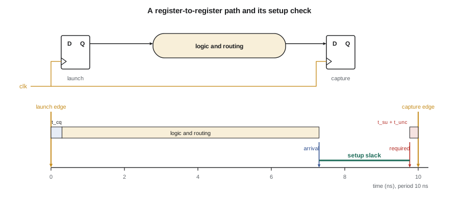
For a register-to-register path, data is launched by a clock edge at the first register, appears at its output after the clock-to-output delay t_cq, propagates through logic and routing, and must arrive at the second register at least the setup time t_su before the next capture edge. The clock itself arrives at the two registers at slightly different times; the clock skew is the capture clock arrival minus the launch clock arrival. Clock uncertainty adds a margin for jitter and other variation. The setup slack is the required time minus the arrival time:
A positive slack means the path meets timing with that much to spare; a negative slack is a violation. The hold check guards against the opposite failure: new data launched by an edge racing through a short path and overwriting the value the capture register is trying to hold after that same edge. It uses the minimum delays:
Setup violations depend on the clock period and can be fixed by slowing the clock; hold violations do not depend on the period at all, so a hold violation means the design fails at any frequency. Positive skew helps setup and hurts hold. FPGA clock networks keep skew small, and the place-and-route tools fix most hold violations automatically by adding routing delay, but hold problems still appear when clocks are routed through general logic or when paths cross between related clocks.
STA analyzes every path at several operating corners, combinations of process, voltage and temperature: slow silicon, low voltage and high temperature for setup, fast silicon, high voltage and low temperature for hold. The results are summarized by the worst negative slack (WNS), the slack of the worst path, and the total negative slack (TNS), the sum over all failing endpoints. WNS shows how far from closure the design is; TNS shows how much of the design is affected.
Constraints
STA can only check requirements it is told about. Timing constraints, written in the widely used SDC format or a close variant, define every clock, the timing of every input and output relative to an external clock, and the paths that need special treatment. Missing constraints are a common cause of hardware that fails despite a clean timing report: a path that is not constrained is not checked.
# primary clocks
create_clock -name clk25  -period 40.000 [get_ports clk25_in]
create_clock -name adc_clk -period 25.000 [get_ports adc_dclk]     ;# 40 MHz from the ADC
# the PLL output (100 MHz) is derived automatically from clk25 by most tools

# the ADC data is launched by the ADC on adc_clk; board and ADC timing from its data sheet
set_input_delay -clock adc_clk -max 6.5 [get_ports {adc_d[*]}]
set_input_delay -clock adc_clk -min 1.0 [get_ports {adc_d[*]}]

# SPI to the ADC: output timing relative to the generated SPI clock
create_generated_clock -name spi_sck -source [get_pins u_spi/sck_reg/C] -divide_by 4 [get_ports spi_sck]
set_output_delay -clock spi_sck -max 5.0 [get_ports spi_mosi]
set_output_delay -clock spi_sck -min -2.0 [get_ports spi_mosi]

# adc_clk and the system clock are unrelated: crossings are handled by the async FIFO
set_clock_groups -asynchronous -group adc_clk -group [get_clocks -of_objects [get_pins u_pll/clkout0]]
# but keep the Gray pointer bits close together (lesson 8)
set_max_delay -datapath_only 8.0 -from [get_cells u_afifo/wgray_reg*] -to [get_cells u_afifo/wgray_s1_reg*]

# the debug UART receive pin is asynchronous and synchronized in the design
set_false_path -from [get_ports uart_rx]
The input delay says how long after the external clock edge the data arrives at the FPGA pin, accounting for the external device's output delay and the board traces, so that STA can check the internal path from the pin to the first register. Output delays work the same way in reverse. A false path declares a path that is never timing-critical, such as a signal into a synchronizer or a static configuration bit, and removes it from analysis. A multicycle path declares that a path has more than one clock period to settle, for example because the destination register is enabled only every fourth cycle. Both are powerful and dangerous: a wrong exception hides a real failure, so every exception in the NS-5 constraint file carries a comment explaining why it is safe, and the review checks each one.
Reading a failing path
The code below repeats the calculation that the timing tool performs, for three paths in Jonah's first build: a state machine's next-state logic, the 32:1 register-read multiplexer of the control interface, and the energy detector, which reads a sample from a block RAM, squares it in a DSP slice and accumulates and compares the result in general logic, all in one cycle. It then repeats the energy path after pipelining it, and finishes with a hold check.
T, UNC = 10.0, 0.15           # 100 MHz period and clock uncertainty (ns)
T_CQ, T_SU, T_H = 0.30, 0.08, 0.05
LUT, CARRY = 0.12, 0.02       # per LUT level; per bit of carry chain

def setup_slack(cells, skew=0.0, t_cq=T_CQ):
    arrival = t_cq + sum(d for _, d in cells)
    required = T + skew - T_SU - UNC
    return required - arrival, arrival

def report(name, cells, skew=0.0, t_cq=T_CQ):
    s, a = setup_slack(cells, skew, t_cq)
    logic = sum(d for n, d in cells if not n.startswith("route"))
    route = a - t_cq - logic
    print(f"  {name:34s} arrival {a:5.2f}  slack {s:+5.2f}  "
          f"(logic {logic:4.2f}, routing {route:4.2f})  {'met' if s >= 0 else 'VIOLATED'}")
    return s

def adder(bits):
    return 0.10 + bits * CARRY

paths = {
    "FSM next state, 3 LUT levels": [("lut", LUT), ("route", 0.35), ("lut", LUT),
                                    ("route", 0.40), ("lut", LUT), ("route", 0.30)],
    "register read mux 32:1": [("lut", LUT), ("route", 0.45), ("wide mux", 0.20),
                               ("route", 0.60), ("lut", LUT), ("route", 0.35)],
    "energy: BRAM->square->acc->compare": [
        ("bram clk-to-out", 1.90 - T_CQ), ("route", 0.90), ("dsp multiply", 3.40),
        ("route", 0.70), ("add48 in fabric", adder(48)), ("route", 0.60),
        ("cmp32", adder(32)), ("lut", LUT), ("route", 0.50), ("lut", LUT), ("route", 0.40)],
}

print("before pipelining, 100 MHz:")
slacks = [report(n, c) for n, c in paths.items()]
wns = min(slacks)
tns = sum(s for s in slacks if s < 0)
print(f"  WNS {wns:+.2f} ns   TNS {tns:+.2f} ns   Fmax of worst path {1000 / (T - wns):.0f} MHz")

stages = {
    "energy stage 1: BRAM out reg -> DSP": ([("route", 0.60)], 0.60),
    "energy stage 2: DSP M reg -> P reg": ([("dsp add48 internal", 1.60)], 0.40),
    "energy stage 3: P reg -> compare": ([("route", 0.60), ("cmp32", adder(32)), ("lut", LUT),
                                          ("route", 0.50), ("lut", LUT), ("route", 0.40)], 0.45),
}
print("after enabling the BRAM output register and the DSP M and P registers:")
slacks = [report(n, c, t_cq=tcq) for n, (c, tcq) in stages.items()]
print(f"  WNS {min(slacks):+.2f} ns, latency +2 cycles, Fmax of worst stage {1000 / (T - min(slacks)):.0f} MHz")

# hold check on a direct flip-flop to flip-flop connection
def hold_slack(t_cq_min, route_min, skew):
    return (t_cq_min + route_min) - (T_H + skew)
for skew in (0.15, 0.45):
    h = hold_slack(0.25, 0.05, skew)
print(f"hold, shift register stage, skew {skew:.2f} ns: slack {h:+.2f} ns {'met' if h >= 0 else 'VIOLATED'}")before pipelining, 100 MHz: FSM next state, 3 LUT levels arrival 1.71 slack +8.06 (logic 0.36, routing 1.05) met register read mux 32:1 arrival 2.14 slack +7.63 (logic 0.44, routing 1.40) met energy: BRAM->square->acc->compare arrival 10.44 slack -0.67 (logic 7.04, routing 3.10) VIOLATED WNS -0.67 ns TNS -0.67 ns Fmax of worst path 94 MHz after enabling the BRAM output register and the DSP M and P registers: energy stage 1: BRAM out reg -> DSP arrival 1.20 slack +8.57 (logic 0.00, routing 0.60) met energy stage 2: DSP M reg -> P reg arrival 2.00 slack +7.77 (logic 1.60, routing 0.00) met energy stage 3: P reg -> compare arrival 2.93 slack +6.84 (logic 0.98, routing 1.50) met WNS +6.84 ns, latency +2 cycles, Fmax of worst stage 316 MHz hold, shift register stage, skew 0.15 ns: slack +0.10 ns met hold, shift register stage, skew 0.45 ns: slack -0.20 ns VIOLATED
The state machine and the register multiplexer pass easily, with more than 7 ns to spare. The energy path fails by 0.67 ns, so the design as a whole would only run at about 94 MHz. The breakdown shows why. Almost all of the delay is in three large blocks used without their pipeline registers: 1.9 ns from the block RAM's unregistered output, 3.4 ns through the DSP slice's unregistered multiplier, and a 48-bit accumulation built from general logic on the carry chain because the code placed it after a combinational comparison that the slice could not absorb. The routing between these blocks adds another 3.1 ns, because block RAM and DSP slices sit in fixed columns and the signals must travel to and from them.
The fix was to rewrite the energy detector as a pipeline: enable the block RAM output register, register the slice's inputs, product and accumulator so that the square and the sum happen inside the slice, and compare the registered accumulator in the following cycle. Each stage is now short; the worst has 6.84 ns of slack, and the only cost is two more cycles of latency on a signal that firmware reads once per frame. The multiply stage inside the slice, from its input registers to its product register, is timed by the slice's own characterization and runs well above 100 MHz.
The hold result is a reminder that hold failures come from skew rather than from slow logic. A direct connection between two flip-flops, such as one stage of a shift register, has almost no delay; with 0.15 ns of clock skew it passes hold by 0.10 ns, but with 0.45 ns of skew, which can happen if a clock is routed on general interconnect instead of a clock network, it fails at any frequency.
Pipelining
Pipelining is the most effective way to close timing. Inserting a register into a long path divides it into two shorter paths, each of which has a full clock period. The throughput stays the same, one result per cycle, and the latency increases by one cycle per register. In an FPGA, pipelining is unusually cheap, because every LUT site already has a flip-flop next to it that is often unused, and block RAM and DSP slices have pipeline registers built in. The general rule for high-performance FPGA design is to pipeline more than seems necessary, especially around block RAM and DSP slices and wherever a signal must cross a large part of the chip.
Pipelining has two costs that the architecture must allow for. Latency grows, which matters in feedback loops: an accumulator whose result is needed in the next cycle cannot simply be pipelined, because the next addition depends on it. And control signals must be delayed by the same number of stages as the data they accompany, a bookkeeping task that valid signals travelling alongside the data, as in the streaming interfaces of lesson 10, make systematic.
Worked problem
How many pipeline stages for a target clock?
A path has 14.0 ns of logic and routing. Each pipeline stage adds register overhead t_cq + t_su + t_unc = 0.53 ns, and each register boundary adds about 0.4 ns of extra routing. If the logic divides evenly, how many stages are needed to run at 250 MHz?
Show solution
- At 250 MHz the period is 4.0 ns. With k stages, each stage carries 14.0/k ns of logic plus 0.93 ns of overhead.
- \[ \frac{14.0}{k} + 0.53 + 0.4 \le 4.0 \;\to\; \frac{14.0}{k} \le 3.07 \;\to\; k \ge 4.56\]
- \[ k = 5: \quad S = 4.0 - 2.8 - 0.93 = +0.27 \text{ ns per stage}\]
Answer: Five stages, each with 2.8 ns of logic and about 0.27 ns of slack.
Retiming and other optimizations
Retiming moves existing registers across combinational logic without changing the circuit's behaviour at its inputs and outputs. If a path has a long stage followed by a short one, moving the register between them backward balances the two. Leiserson and Saxe formalized retiming in 1991, and FPGA synthesis and implementation tools can perform it automatically when it is enabled, although it is limited by registers with resets or initial values, by registers that are read by other logic, and by the boundaries of DSP slices and block RAM. A useful style is to write a few extra registers at the end of a long combinational block and let retiming push them into the logic, which gives the tool freedom without the designer having to find the best cut.
Other techniques address specific causes of delay. High fanout, one register driving hundreds of loads, makes a long routing tree; duplicating the register, so that each copy drives a subset, shortens it, and tools do this automatically with a fanout limit. Reducing logic levels helps, for example by replacing a long priority chain with a balanced case statement or by precomputing a condition one cycle early. Choosing a better architecture helps most of all: the energy path's real fault was not a lack of registers but a structure that kept the arithmetic outside the DSP slice.
Floorplanning, constraining blocks to regions of the chip, can help large designs by keeping related logic together, but it is a last resort in mid-sized designs, because a poor floorplan easily makes timing worse. The place-and-route tools also offer strategies that spend more run time on optimization, and running several strategies or seeds in parallel is a common way to close the last fraction of a nanosecond. Relying on that habitually is a sign that the design has too little margin.
A closure method
Experienced designers follow a fixed order when a design fails timing. First, check the constraints: is the clock correct, are all clocks and inputs constrained, and are the failing paths real or the result of a missing exception such as an unconstrained crossing? Second, look at the worst paths and classify them by cause: too many logic levels, a hard block used without its registers, long routes between fixed blocks, high fanout, or a crossing that should not be timed. Third, fix the cause in the RTL, usually by pipelining or restructuring, rather than tuning tool options. Fourth, keep margin: Northway Sensing requires at least 0.3 ns of positive slack at the slow corner on every build, so that small changes and tool updates do not break timing in the field update a year later.
Timing should be considered from the architecture onward, not discovered at the end. The estimate of lesson 1 already chose a 100 MHz clock with 50 cycles per output, which gives the MAC engine slack to spare; register boundaries between modules, recommended in lesson 3, keep timing problems local; and the memory and DSP templates of lessons 6 and 7 were written with their pipeline registers from the start. The energy detector failed precisely because it was written quickly, outside those habits.
Common mistakes
MistakeTreating a clean timing report as proof when constraints are incomplete.
InsteadCheck that every clock, input, output and exception is constrained; unconstrained paths are not checked.
MistakeFixing hold violations by slowing the clock.
InsteadHold slack does not depend on the period; fix the skew or add delay on the short path.
MistakeAdding false paths or multicycle paths to make violations disappear.
InsteadUse exceptions only where the design guarantees them, and document why each is safe.
MistakeUsing block RAM and DSP slices without their internal registers.
InsteadEnable their pipeline registers; they are the main source of fast paths in an FPGA.
MistakePipelining a feedback loop without changing the algorithm.
InsteadAccount for the added latency in loops, or restructure so the loop fits in one cycle.
Summary and key terms
- STA checks every timing path without simulation, at slow and fast operating corners.
- Setup slack = (T + skew − t_su − t_unc) − (t_cq + logic + routing); hold slack uses minimum delays and does not depend on T.
- WNS and TNS summarize how far and how widely a design misses timing.
- Constraints define clocks, input and output delays, asynchronous groups and exceptions; missing constraints hide failures.
- Pipelining, retiming, fanout control, fewer logic levels and better architectures close timing.
- The NS-5 energy path failed by 0.67 ns and passed with 6.84 ns of slack after using the block RAM and DSP registers.
- Static timing analysis (STA)
- Verification of timing by computing delays along every path rather than by simulation.
- Slack
- The difference between the required time and the arrival time on a path; negative slack is a violation.
- Clock skew
- The difference in arrival times of a clock edge at two registers.
- Clock uncertainty
- A margin applied to timing checks to account for jitter and other clock variation.
- Worst negative slack (WNS)
- The most negative slack among all timing endpoints.
- False path
- A path declared not to require timing analysis.
- Multicycle path
- A path allowed more than one clock period to propagate.
- Retiming
- Moving registers across combinational logic to balance path delays without changing behaviour.
Practice problems
Work each problem on paper first, then reveal the answer to check.
A path at 125 MHz has t_cq = 0.3 ns, logic and routing of 7.1 ns, t_su = 0.08 ns, uncertainty 0.15 ns and zero skew. What is the setup slack?
Show answer
8.0 − 0.08 − 0.15 − 7.4 = +0.37 ns.
What is the hold slack with t_cq,min = 0.25 ns, a route of 0.05 ns, t_h = 0.05 ns and skew 0.30 ns?
Show answer
0.30 − 0.35 = −0.05 ns, a violation.
A register drives 600 loads and its path fails by 0.4 ns, almost all in routing. What should be tried first?
Show answer
Duplicate the register, with a fanout limit or by hand, so each copy drives fewer loads.
Why is a false path on a synchronizer input correct, but a false path on the energy path wrong?
Show answer
The synchronizer is designed to tolerate any arrival time; the energy path's result is used every cycle and must settle.
Lesson quiz · 5 questions
Score 60% or more to complete this lesson.
Create a free account to save your progress, take quizzes and earn a certificate.