
CMP-450 · Lesson 8 of 12 · 24 min
Clock domains and CDC: synchronizers, async FIFOs, linking to ELE-210 MTBF
Everything so far has assumed one clock. Real designs have several. The NS-5 front end receives samples on the ADC's own 40 MHz data clock, processes them on a 100 MHz system clock, talks to the processor on the interconnect's clock, and samples a frame-sync pulse from the radar that is synchronous to nothing at all. Every signal that passes between unrelated clocks is a clock-domain crossing (CDC), and CDC bugs are among the most dangerous in digital design: they pass every simulation, they appear rarely and randomly in hardware, and they can take months to diagnose. This lesson develops the standard crossing circuits and the reasoning that makes them safe.
The ELE-210 lesson on timing and clocking introduced metastability and the synchronizer MTBF formula. This lesson builds on that: it applies the formula to FPGA design decisions, then moves from single bits to the crossings that real designs need, pulses, handshakes, buses and FIFOs.
Why crossings fail
A flip-flop guarantees a clean output only if its input is stable for the setup time before the clock edge and the hold time after it. When the input comes from a different clock domain, there is no fixed timing relationship, so sooner or later the input will change inside that window. The flip-flop can then become metastable, its output hovering between 0 and 1 for an unpredictable time before resolving to one or the other. The probability that it is still unresolved after a time t falls exponentially, with a time constant τ that is a property of the flip-flop. As ELE-210 showed, the mean time between failures of a synchronizer is:
where t_r is the resolution time allowed before the output is used, f_clk is the receiving clock frequency, f_data is the rate at which the asynchronous input changes, and T_0 is a second flip-flop constant that sets the width of the vulnerable window. Because t_r is in the exponent, small changes in it have enormous effects, which is the whole basis of synchronizer design.
Metastability is not the only failure. If an asynchronous signal fans out to several flip-flops, each may see it on a different side of the edge, so in the same cycle part of the logic sees the old value and part sees the new. A state machine whose next-state logic reads an unsynchronized input can move to an illegal combination of states this way, even if no flip-flop ever goes metastable. Both problems have the same cure: every asynchronous input passes through exactly one synchronizer, and only the synchronizer's output is used.
The two-flip-flop synchronizer
The basic synchronizer is two flip-flops in series on the receiving clock with nothing between them. The first may go metastable; it has almost a whole clock period to resolve before the second samples it. The resolution time is the clock period minus the first flip-flop's clock-to-output delay, the second's setup time and the routing between them, which is why the two must be placed next to each other. FPGA tools recognize synchronizer chains marked with an attribute, keep them out of shift-register LUTs, place them together and exclude them from optimizations that would move logic between them.
module sync2 #(parameter int STAGES = 2) (
    input  logic clk,          // receiving clock
    input  logic d_async,      // from another domain, registered there
    output logic q
);
    (* async_reg = "true" *) logic [STAGES-1:0] s;   // keep together, no SRL
    always_ff @(posedge clk)
        s <= {s[STAGES-2:0], d_async};
    assign q = s[STAGES-1];
endmodule
The source signal must be driven directly by a flip-flop in its own domain, never by combinational logic. Combinational logic can glitch when its inputs change, and a glitch that the receiving domain happens to sample is captured as a real pulse. This is one of the rules that CDC checking tools enforce, along with the rule that nothing reads the first stage of a synchronizer.
How much resolution time is enough?
The code below applies the MTBF formula, with the same illustrative constants as ELE-210 (τ = 50 ps, T_0 = 20 ps) and NS-5 timing values, to four cases: a signal used directly by logic with only 0.8 ns of slack, a two-flip-flop synchronizer at 100 MHz, the same at 400 MHz, and three flip-flops at 400 MHz. It then scales the 400 MHz cases to a fleet. Finally it shows why a multi-bit counter must be Gray coded before it crosses.
import math, itertools

TAU, T0 = 50e-12, 20e-12             # same illustrative constants as ELE-210 lesson 11

def log10_mtbf(t_r, f_clk, f_data):
    """log10 of MTBF in seconds: e^(t_r/tau) / (T0 f_clk f_data)"""
    return t_r / TAU / math.log(10) - math.log10(T0 * f_clk * f_data)

def show(name, t_r, f_clk, f_data=2e6):
    lg = log10_mtbf(t_r, f_clk, f_data)
    if lg < 7:
        text = f"{10**lg:,.0f} s ({10**lg / 60:,.0f} min)"
    else:
        text = f"10^{lg:.0f} s"
    print(f"{name:44s} t_r = {t_r*1e9:5.2f} ns   MTBF = {text}")
    return lg

T_CQ, T_SU, T_ROUTE = 0.30e-9, 0.08e-9, 0.25e-9
show("no synchronizer, 0.8 ns slack, 100 MHz", 0.8e-9, 100e6)
lg2 = show("two flip-flops, 100 MHz", 10e-9 - T_CQ - T_SU - T_ROUTE, 100e6)
lg4 = show("two flip-flops, 400 MHz", 2.5e-9 - T_CQ - T_SU - T_ROUTE, 400e6)
lg3 = show("three flip-flops, 400 MHz", 2 * (2.5e-9 - T_CQ - T_SU - T_ROUTE), 400e6)

units, syncs = 5000, 40                     # a fleet of boards, synchronizers per board
n = units * syncs
print(f"fleet of {units} units x {syncs} synchronizers at 400 MHz:")
print(f"  two flip-flops:   one failure somewhere every {10**lg4 / n / 86400:,.0f} days")
print(f"  three flip-flops: one failure somewhere every 10^{lg3 - math.log10(n * 3.156e7):.0f} years")

# why multi-bit counters must be Gray coded before crossing
gray = lambda b: b ^ (b >> 1)
def bad_samples(a, b, w=4, code=lambda v: v):
    """values a receiver can capture if each changing bit is caught old or new"""
    ca, cb = code(a), code(b)
    diff = [i for i in range(w) if (ca ^ cb) >> i & 1]
    seen = set()
    for pick in itertools.product([0, 1], repeat=len(diff)):
        v = ca
        for bit, p in zip(diff, pick):
            if p:
                v ^= 1 << bit
        seen.add(v)
    legal = {ca, cb}
    return len(seen - legal)

print(f"binary 7 -> 8: {bad_samples(7, 8)} wrong values possible;"
      f" Gray 7 -> 8: {bad_samples(7, 8, code=gray)}")

for depth in (8, 6):
    codes = [gray(i) for i in range(depth)]
    steps = [bin(codes[i] ^ codes[(i + 1) % depth]).count("1") for i in range(depth)]
print(f"Gray sequence of length {depth}: bits changing at each step {steps}")no synchronizer, 0.8 ns slack, 100 MHz t_r = 0.80 ns MTBF = 2,222 s (37 min) two flip-flops, 100 MHz t_r = 9.37 ns MTBF = 10^78 s two flip-flops, 400 MHz t_r = 1.87 ns MTBF = 10^12 s three flip-flops, 400 MHz t_r = 3.74 ns MTBF = 10^28 s fleet of 5000 units x 40 synchronizers at 400 MHz: two flip-flops: one failure somewhere every 63 days three flip-flops: one failure somewhere every 10^15 years binary 7 -> 8: 14 wrong values possible; Gray 7 -> 8: 0 Gray sequence of length 8: bits changing at each step [1, 1, 1, 1, 1, 1, 1, 1] Gray sequence of length 6: bits changing at each step [1, 1, 1, 1, 1, 3]
Without a synchronizer, the frame-sync input would cause a failure about every 37 minutes. Adding a second flip-flop at 100 MHz raises the resolution time to 9.37 ns and the MTBF to about 10^78 seconds, a number with no practical meaning except that this crossing will never fail. At 400 MHz the period is a quarter as long and the MTBF falls to about 10^12 seconds, roughly 35,000 years for one synchronizer. That sounds safe until it is multiplied out: 5,000 units with 40 such synchronizers each would see a failure somewhere in the fleet about every two months. A third flip-flop restores an astronomical margin. The lesson is that MTBF must be computed for the product, not the circuit, and that fast clocks need longer synchronizers.
Worked problem
Choosing synchronizer length for a fast clock
A design samples an asynchronous input at 500 MHz with t_cq + t_su + routing = 0.6 ns. With τ = 50 ps and T_0 = 20 ps, and an input that changes at 1 MHz, what is the MTBF of a two-stage synchronizer?
Show solution
- \[ t_r = 2.0 - 0.6 = 1.4 \text{ ns}, \quad \frac{t_r}{\tau} = 28\]
- \[ T_0 f_{clk} f_{data} = 20 \times 10^{-12} \times 5 \times 10^{8} \times 10^{6} = 10^{4}\]
- \[ \mathrm{MTBF} = \frac{e^{28}}{10^{4}} \approx \frac{1.45 \times 10^{12}}{10^{4}} = 1.45 \times 10^{8} \text{ s}\]
- That is about 4.6 years for one synchronizer, too short for a product. A third stage adds 1.4 ns more and multiplies the MTBF by e^28.
Answer: About 1.5 × 10^8 s, or 4.6 years; use three stages at this clock rate.
Crossing a pulse
A two-flip-flop synchronizer passes a level that stays stable for at least a couple of receiving-clock cycles. A single-cycle pulse from a fast domain may fall between two edges of a slow clock and vanish. The standard pulse synchronizer converts the pulse to a toggle in the source domain, a flip-flop that changes state on every pulse, synchronizes the level, and detects each change in the destination domain with an XOR of the last two stages. Each source pulse produces exactly one destination pulse, provided pulses are spaced far enough apart for each toggle to be seen, about three destination cycles.
// source domain: turn each pulse into a level change
always_ff @(posedge clk_a) if (pulse_a) tog_a <= ~tog_a;

// destination domain: synchronize the level, then detect each change
(* async_reg = "true" *) logic [2:0] s;
always_ff @(posedge clk_b) s <= {s[1:0], tog_a};
assign pulse_b = s[2] ^ s[1];
When the pulses can come faster, or when data must travel with the event, a handshake is used. The source places data on a bus, holds it stable and raises a request; the destination synchronizes the request, captures the data, which has been stable for several cycles, and raises an acknowledgement; the source synchronizes the acknowledgement and lowers the request, and so on. The four-phase handshake costs several cycles in each direction per transfer, so it suits configuration registers and occasional events. The NS-5 uses it for the gain and offset settings that firmware writes to the ADC-domain logic.
Why buses cannot be synchronized bit by bit
Passing each bit of a multi-bit value through its own synchronizer does not work. When several bits change at once, each synchronizer may resolve its bit differently, so the receiver can capture a mixture of old and new bits that was never present in the source. The code shows the extreme case: a binary counter moving from 7 to 8 changes all four bits, and a receiver catching each bit either old or new can see 14 wrong values, anything from 0 to 15 except 7 and 8. In Gray code, successive values differ in exactly one bit, so the receiver sees either the old value or the new one and nothing else.
There are therefore three correct ways to cross a bus: hold it stable and send a synchronized control signal that says when to capture it, as the handshake does; encode it so that only one bit changes per step, which works for counters; or put it through an asynchronous FIFO, which combines both ideas.
The asynchronous FIFO
An asynchronous FIFO is the general-purpose crossing for data streams. Its memory is a dual-port RAM with the write port on the source clock and the read port on the destination clock. The write pointer lives in the write domain and the read pointer in the read domain. To generate full, the write side needs the read pointer; to generate empty, the read side needs the write pointer. Each pointer is converted to Gray code in its own domain, registered, and passed through a synchronizer to the other side, where it is compared with the local pointer, also in Gray code. This is the design described by Clifford Cummings in 2002, which remains the reference implementation.
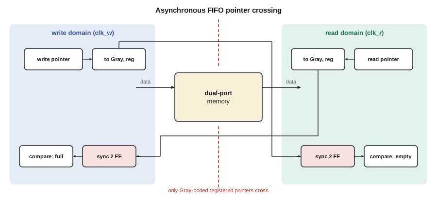
// write domain (clk_w): binary and Gray write pointers, AW+1 bits each
always_ff @(posedge clk_w or posedge rst_w)
    if (rst_w) begin wbin <= '0; wgray <= '0; end
    else if (wr && !full) begin
        wbin  <= wbin + 1'b1;
        wgray <= (wbin + 1'b1) ^ ((wbin + 1'b1) >> 1);   // registered Gray code
    end

// read pointer, synchronized into the write domain
(* async_reg = "true" *) logic [AW:0] rgray_s1, rgray_s2;
always_ff @(posedge clk_w) begin rgray_s1 <= rgray; rgray_s2 <= rgray_s1; end

// full: Gray write pointer equals the synchronized read pointer with its top two bits inverted
assign full = (wgray == {~rgray_s2[AW:AW-1], rgray_s2[AW-2:0]});

// read domain (clk_r) mirrors this: rgray, wgray synchronized into clk_r, and
assign empty = (rgray == wgray_s2);
The full test looks unusual because the pointers carry the extra wrap bit of lesson 7 and are in Gray code. In Gray code, the value half-way round the sequence, which is what a pointer that has lapped the other looks like, differs in the top two bits, not just the top one. The logic is subtle enough that teams use a proven implementation rather than writing a new one, and verify it with formal tools, but every designer should understand why it works.
Three properties make the asynchronous FIFO safe. Only one bit of each pointer changes per increment, so a synchronized pointer is always either the current value or a recent one. A stale pointer is always conservative: the write side sees the read pointer late, so it may think the FIFO is fuller than it is but never emptier, and the read side may think it is emptier than it is but never fuller. Full and empty are therefore asserted on time and deasserted a few cycles late, which costs a little throughput but never loses data. And the depth must be a power of two, because a Gray sequence wraps with a single-bit change only when its length is a power of two; the code shows that a six-entry sequence changes three bits at the wrap.
The synchronization delay also affects sizing. The write side learns about reads two or three of its cycles late, so the FIFO must be a few entries deeper than the rate calculation of lesson 7 suggests. The NS-5 ADC crossing writes one 48-bit word, all four channels, at 2 MHz from the 40 MHz domain and reads it at up to 100 MHz, so it never fills in normal operation; its depth of 512 comes from using one block RAM, and it absorbs the read side's pause while the processor resets the front end.
Resets across domains
Lesson 3 recommended asserting reset asynchronously and releasing it synchronously. The circuit that does this is a reset synchronizer: two flip-flops whose asynchronous clear is driven by the raw reset, with a constant 1 shifted in. When reset is asserted, both clear at once; when it is released, the 1 takes two clock edges to reach the output, so the domain leaves reset cleanly on an edge. Each clock domain needs its own reset synchronizer, and blocks that cross between domains, such as asynchronous FIFOs, must be reset in both domains with an agreed sequence so that neither side sees a half-reset partner.
module reset_sync (input logic clk, rst_async_n, output logic rst_n);
    (* async_reg = "true" *) logic s1, s2;
    always_ff @(posedge clk or negedge rst_async_n)
        if (!rst_async_n) begin s1 <= 1'b0; s2 <= 1'b0; end
        else              begin s1 <= 1'b1; s2 <= s1;   end
    assign rst_n = s2;
endmodule
Clocks, constraints and checking
Not every pair of clocks is asynchronous. Clocks generated from the same source by a phase-locked loop, such as a 100 MHz and a 200 MHz clock from one PLL, have a fixed phase relationship, and paths between them can be timed normally by static timing analysis. Clocks from different sources, or with an unknown relationship, must be declared asynchronous to the timing tool, so that it does not try to time paths it cannot meaningfully analyze. Declaring them asynchronous is not the same as making the crossings safe: the tool simply stops checking, so every path between those clocks must go through a proper crossing circuit. For Gray-coded pointer buses, a maximum-delay constraint between the source and destination registers keeps the bits' skew below one destination clock period, preserving the one-bit-change property after routing.
Static timing analysis and simulation both miss CDC problems: timing analysis because the crossing paths are excluded, simulation because the simulator's flip-flops never go metastable and its clocks have a fixed relationship. Structural CDC checking tools fill the gap. They find every crossing in the netlist and check that each one goes through a recognized synchronizer, that multi-bit crossings are Gray coded or qualified by a synchronized control signal, that no logic sits between synchronizer stages, and that nothing fans out from an unsynchronized signal. Ines's review checklist for the NS-5 requires a clean CDC report with every waived crossing explained in writing.
Finally, designs should not create clock domains unnecessarily. A slow process that only needs to run every fourth cycle should use a clock enable on the main clock, not a divided clock: a clock built from logic has unpredictable skew, and every path to and from it becomes a crossing. Gated clocks, created by ANDing a clock with an enable, have the same problems and can glitch. FPGAs provide dedicated clock buffers with enables for the rare cases where stopping a clock really is needed to save power.
Common mistakes
MistakePassing a multi-bit binary value through a synchronizer on each bit.
InsteadUse Gray code for counters, a handshake for held data, or an asynchronous FIFO for streams.
MistakeDriving a synchronizer from combinational logic in the source domain.
InsteadRegister the signal in the source domain so it cannot glitch.
MistakeDeclaring clocks asynchronous and assuming the crossings are now safe.
InsteadAsynchronous declarations stop timing checks; every crossing still needs a proper circuit and a CDC check.
MistakeUsing a non-power-of-two depth for an asynchronous FIFO with Gray pointers.
InsteadMake the depth a power of two so the Gray sequence wraps with one bit changing.
MistakeDividing a clock with logic to slow part of the design down.
InsteadUse a clock enable on the main clock, or a dedicated clock resource.
Summary and key terms
- A clock-domain crossing risks metastability and inconsistent sampling; every asynchronous signal needs exactly one synchronizer.
- MTBF = e^(t_r/τ)/(T_0 f_clk f_data); resolution time in the exponent dominates.
- Two flip-flops suffice at 100 MHz; fast clocks and large fleets may need three.
- Pulses cross as toggles; held data crosses with a four-phase handshake.
- Buses cross only in Gray code, with a qualifying control signal or through an asynchronous FIFO.
- Asynchronous FIFOs synchronize registered Gray pointers, give conservative full and empty, and need power-of-two depths.
- Reset synchronizers, asynchronous clock constraints, CDC checking tools and clock enables complete safe multi-clock design.
- Clock-domain crossing (CDC)
- A signal path from a register on one clock to a register on an unrelated clock.
- Metastability
- An unstable state of a flip-flop whose input changed inside its setup and hold window.
- Synchronizer
- A chain of flip-flops on the receiving clock that allows a metastable value time to resolve.
- Resolution time
- The time a synchronizer stage has for a metastable output to resolve before it is sampled.
- Toggle synchronizer
- A pulse crossing circuit that converts pulses to level changes and detects the changes in the destination domain.
- Four-phase handshake
- A request and acknowledge protocol that transfers held data across clock domains.
- Gray code
- A binary code in which successive values differ in exactly one bit.
- Asynchronous FIFO
- A FIFO with read and write ports on different clocks, using synchronized Gray-coded pointers.
Practice problems
Work each problem on paper first, then reveal the answer to check.
An unsynchronized input feeds logic with 1.2 ns of slack at 100 MHz, τ = 50 ps, T_0 = 20 ps, f_data = 2 MHz. Estimate the MTBF.
Show answer
e^24 / 4,000 ≈ 2.65 × 10^10 / 4,000 ≈ 6.6 × 10^6 s, about 77 days.
What is the Gray code of binary 1011?
Show answer
1011 XOR 0101 = 1110.
A pulse synchronizer receives source pulses every cycle of a 200 MHz clock into a 50 MHz domain. What goes wrong?
Show answer
The toggle changes faster than the destination can sample it, so pulses are lost; use a FIFO or a counter instead.
Why does a stale read pointer never make the write side overflow the FIFO?
Show answer
A stale read pointer makes the FIFO look fuller than it is, so full is asserted early, never late.
Lesson quiz · 5 questions
Score 60% or more to complete this lesson.
Create a free account to save your progress, take quizzes and earn a certificate.