
CMP-350 · Lesson 4 of 12 · 19 min
The CMOS inverter: transfer curve and noise margins
The inverter is the simplest CMOS gate and the template for all the others. One n-channel transistor connects the output to ground, one p-channel transistor connects it to the supply, and both gates are tied to the input. When the input is low, the n-channel device is off and the p-channel device is on, pulling the output to V_DD. When the input is high, the roles reverse and the output is pulled to ground. In either steady state one transistor is off, so no current flows from supply to ground. This lesson studies the inverter's voltage transfer characteristic, the curve of output voltage against input voltage, and uses it to define the switching threshold, the logic levels and the noise margins that make digital circuits robust.
Ines brings the topic to the bench with a practical question. The NS-5 microcontroller's datasheet promises that any input above 0.7 V_DD reads as a 1 and any input below 0.3 V_DD reads as a 0, and that its outputs reach within 0.4 V of the rails. Where do those numbers come from, and how much noise can a signal crossing the board pick up before a bit flips? The answers come straight from the inverter, because every input pin starts with one.
How the inverter works
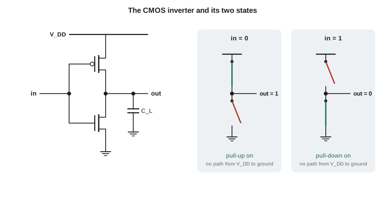
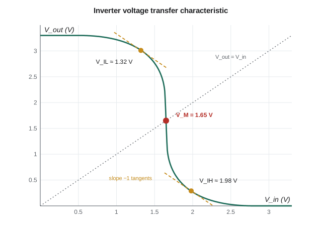
Treating each transistor as a switch gives the logic function, but the interesting behaviour lies between the extremes. As the input rises from 0 V, nothing happens until it passes the n-channel threshold V_tn. Then the n-channel device begins to conduct while the p-channel device is still strongly on, and the output starts to fall slightly. Near the middle of the range both transistors are in saturation and the output swings steeply from high to low for a small change in input; this is the region of high gain. As the input approaches V_DD − |V_tp|, the p-channel device turns off and the output settles at 0 V. The result is the S-shaped transfer curve below.
The switching threshold
The switching threshold V_M is the input voltage at which the output equals the input, where the curve crosses the diagonal. At that point both transistors are in saturation and carry the same current. Setting the two saturation currents equal gives V_M in terms of the threshold voltages and the ratio of transistor strengths.
If the n- and p-channel devices have the same strength, r = 1 and, with equal threshold magnitudes, V_M sits at exactly V_DD/2. Because holes are less mobile, equal strength requires the p-channel device to be wider, by the ratio of k_n to k_p. A designer can deliberately skew V_M: a stronger p-channel device moves it up, a stronger n-channel device moves it down. Skewed inverters are used to detect a rising or falling edge early, and the input buffers of microcontroller pins are often designed with a Schmitt trigger, described below, rather than a single fixed threshold.
Worked problem
Switching threshold of a minimum inverter
A process has k_n = 300 µA/V², k_p = 120 µA/V² and |V_t| = 0.5 V for both types, on a 3.3 V supply. Find V_M for an inverter with equal widths, W/L = 2 for both devices, and the width ratio needed to centre V_M at 1.65 V.
Show solution
- \[ r = \sqrt{\frac{120 \times 2}{300 \times 2}} = 0.632\]
- \[ V_M = \frac{0.5 + 0.632 \times (3.3 - 0.5)}{1 + 0.632} = \frac{2.27}{1.632} = 1.39\ \text{V}\]
- \[ \text{for } r = 1: \frac{(W/L)_p}{(W/L)_n} = \frac{k_n}{k_p} = \frac{300}{120} = 2.5\]
Answer: With equal widths the threshold falls to about 1.39 V, below mid-supply, because the n-channel device is stronger. Making the p-channel device 2.5 times wider, W/L = 5 against 2, centres V_M at 1.65 V.
Logic levels and noise margins
A digital system must tolerate noise. Signals pick up crosstalk from neighbouring wires, ground bounce when many outputs switch, and supply ripple. The transfer curve shows how much noise a gate can absorb. The points where its slope equals −1 mark where the gain changes from less than one, where noise is attenuated, to greater than one, where it is amplified. The input voltages at those points define the input thresholds: V_IL, the highest input voltage guaranteed to be read as low, and V_IH, the lowest input voltage guaranteed to be read as high. Between them is a forbidden zone where the output is not a valid logic level.
The output levels V_OH and V_OL are the voltages a gate guarantees to produce for a high and a low. Noise margins compare what one gate guarantees to produce with what the next gate needs. The low noise margin is the amount by which a valid low output can be pushed up by noise before the next gate stops reading it as low; the high noise margin is the corresponding figure for a high output.
Datasheet values are deliberately more conservative than an ideal inverter's unity-gain points, because they must hold across process, voltage and temperature and include the loading on the output. A typical 3.3 V CMOS microcontroller specifies V_IH as 0.7 V_DD (2.31 V), V_IL as 0.3 V_DD (0.99 V), V_OH as V_DD − 0.4 V (2.9 V) at a few milliamps of load, and V_OL as 0.4 V. Those give noise margins of about 0.59 V in each direction. An unloaded CMOS output swings all the way to the rails, giving even bigger margins; the 0.4 V figures allow for the voltage dropped across the output transistor's on-resistance when it supplies current, as lesson 3 calculated.
| Parameter | Typical 3.3 V CMOS | Meaning |
|---|---|---|
| V_IH (min) | 0.7 V_DD = 2.31 V | Lowest input guaranteed to read high |
| V_IL (max) | 0.3 V_DD = 0.99 V | Highest input guaranteed to read low |
| V_OH (min) | V_DD − 0.4 V = 2.9 V at the rated current | Lowest guaranteed high output |
| V_OL (max) | 0.4 V at the rated current | Highest guaranteed low output |
| NM_H | 2.9 − 2.31 = 0.59 V | Noise a high level can tolerate |
| NM_L | 0.99 − 0.4 = 0.59 V | Noise a low level can tolerate |
Regeneration: why digital signals stay clean
The high gain in the middle of the transfer curve gives CMOS logic a property analog circuits lack: regeneration. Suppose a signal arrives slightly degraded, say a high level of 2.8 V instead of 3.3 V. The first gate's output is still very close to 0 V because the input is far into the low-gain region, and the second gate restores a clean 3.3 V. A chain of gates therefore pushes noisy signals back toward the rails at every stage instead of accumulating the noise. As long as the noise at each stage stays within the noise margin, information passes through any number of gates without error. This is the deep reason digital electronics scales to billions of gates.
Static and short-circuit current
In either steady state an ideal CMOS inverter draws no current, apart from leakage. During a transition, though, there is a brief interval when the input is between V_tn and V_DD − |V_tp| and both transistors conduct, so current flows straight from supply to ground. This short-circuit current is usually a small fraction of the total switching power, a few percent to perhaps twenty percent, provided input edges are fast. Slow input edges make it much worse, because the gate spends longer in the middle region. That is why an input pin left floating, or driven by a slowly rising signal such as an RC delay, can make a chip draw unexpected current: its input buffer sits in the conducting region. Part of the hidden sleep current that CMP-315 tracked down on the NS-4 came from unused pins left floating, and a single floating input can draw tens of microamps for exactly this reason; lesson 7 returns to the numbers.
Schmitt triggers: hysteresis at the input
A slowly changing or noisy input can cross the switching threshold several times as it passes through, making the output chatter. A Schmitt trigger adds hysteresis: the threshold for a rising input, V_T+, is higher than the threshold for a falling input, V_T−. Once the input has crossed V_T+ and the output has switched, it must fall all the way below V_T− before the output switches back. Noise smaller than the hysteresis band cannot cause extra transitions. CMOS Schmitt triggers use extra transistors that feed the output back to shift the threshold. CMP-240 built one from an op-amp for the NS-4's low-battery detector; many microcontroller pins can enable a Schmitt input buffer, and Ines turns it on for the NS-5's tamper switch input, which is connected through a long cable and an RC filter.
Computing the transfer curve
The program below finds the inverter's output for each input voltage by balancing the n- and p-channel currents with a bisection search, using the long-channel model from lesson 3 with a small channel-length modulation term so the steep region has finite gain. It then locates the unity-gain points and reports the switching threshold, the logic levels and the noise margins for the balanced inverter from the example.
VDD = 3.3
kn, kp = 300e-6, 120e-6       # A/V^2 (process parameters)
WLn, WLp = 2.0, 5.0           # sizing chosen so kn*WLn = kp*WLp
Vtn, Vtp = 0.5, 0.5           # magnitudes of thresholds
lam = 0.05                    # channel-length modulation, 1/V

def ids(k, wl, vgs, vds, vt):
    vov = vgs - vt
    if vov <= 0 or vds <= 0:
        return 0.0
    if vds < vov:
        return k * wl * (vov * vds - 0.5 * vds * vds) * (1 + lam * vds)
    return 0.5 * k * wl * vov * vov * (1 + lam * vds)

def vout(vin):
    lo, hi = 0.0, VDD
    for _ in range(60):
        mid = (lo + hi) / 2
        i_n = ids(kn, WLn, vin, mid, Vtn)
        i_p = ids(kp, WLp, VDD - vin, VDD - mid, Vtp)
        if i_n > i_p:
            hi = mid
        else:
            lo = mid
    return (lo + hi) / 2

N = 3301
vins = [VDD * i / (N - 1) for i in range(N)]
vouts = [vout(v) for v in vins]
slopes = [(vouts[i + 1] - vouts[i]) / (vins[i + 1] - vins[i]) for i in range(N - 1)]
VIL = next(vins[i] for i, s in enumerate(slopes) if s <= -1)
VIH = next(vins[i] for i in range(N - 2, -1, -1) if slopes[i] <= -1)
VM = next(vins[i] for i in range(N) if vouts[i] <= vins[i])
VOH, VOL = vout(VIL), vout(VIH)
print(f"switching threshold VM = {VM:.2f} V")
print(f"VIL = {VIL:.2f} V, VOH at VIL = {VOH:.2f} V")
print(f"VIH = {VIH:.2f} V, VOL at VIH = {VOL:.2f} V")
print(f"NM_L = VIL - VOL = {VIL - VOL:.2f} V")
print(f"NM_H = VOH - VIH = {VOH - VIH:.2f} V")
print(f"peak gain = {min(slopes):.1f}")switching threshold VM = 1.65 V VIL = 1.32 V, VOH at VIL = 3.01 V VIH = 1.98 V, VOL at VIH = 0.29 V NM_L = VIL - VOL = 1.03 V NM_H = VOH - VIH = 1.04 V peak gain = -37.7
The balanced inverter switches at 1.65 V, with unity-gain points at about 1.32 V and 1.98 V and noise margins just over 1 V on each side. That is better than the 0.59 V a datasheet promises, because the simulation has no load current and no process or temperature spread. The peak gain of about −38 shows how steep the middle of the curve is. Change WLp to 2.0 in the code and the threshold drops to about 1.39 V, matching the worked example, and the low noise margin shrinks.
Common mistakes
MistakeTaking V_M as V_DD/2 for any inverter.
InsteadV_M depends on the strength ratio of the transistors; equal widths put it below mid-supply.
MistakeConfusing input thresholds with output levels.
InsteadV_IH and V_IL describe what an input needs; V_OH and V_OL describe what an output guarantees. Noise margins compare the two.
MistakeLeaving CMOS inputs floating.
InsteadA floating input can sit near V_M, where both transistors conduct and the gate draws current or oscillates; tie it with a pull resistor or drive it.
MistakeDriving a CMOS input with a slow RC edge without hysteresis.
InsteadSlow edges cause short-circuit current and chatter; use a Schmitt-trigger input.
Summary and key terms
- A CMOS inverter pulls the output up with a p-channel device and down with an n-channel device; one is always off.
- The transfer curve has low-gain regions at each end and a high-gain region in the middle.
- The switching threshold V_M depends on the ratio of transistor strengths; balancing it needs a wider p-channel device.
- V_IL and V_IH are set where the slope is −1; V_OH and V_OL are what an output guarantees.
- Noise margins NM_L = V_IL − V_OL and NM_H = V_OH − V_IH measure tolerance to noise.
- High gain gives regeneration, so clean levels are restored at every stage.
- Short-circuit current flows during transitions and grows with slow edges.
- Schmitt triggers add hysteresis to reject noise on slow inputs.
- Voltage transfer characteristic
- The curve of a gate’s output voltage against its input voltage.
- Switching threshold
- The input voltage at which output equals input, V_M.
- V_IH
- The minimum input voltage guaranteed to be read as high.
- V_IL
- The maximum input voltage guaranteed to be read as low.
- Noise margin
- The amount of noise a logic level can tolerate before it is misread.
- Regeneration
- The restoration of degraded logic levels by the gain of successive gates.
- Short-circuit current
- Current flowing directly from supply to ground while both transistors conduct during a transition.
- Hysteresis
- Different thresholds for rising and falling inputs, used to reject noise.
Practice problems
Work each problem on paper first, then reveal the answer to check.
A driver guarantees V_OL = 0.3 V and V_OH = 3.0 V; a receiver needs V_IL = 1.0 V and V_IH = 2.3 V. What are the noise margins?
Show answer
NM_L = 1.0 − 0.3 = 0.7 V; NM_H = 3.0 − 2.3 = 0.7 V.
If k_n = 2.5 k_p, what width ratio of p- to n-channel devices balances an inverter with equal thresholds?
Show answer
2.5 : 1.
Why does a slowly rising input increase an inverter’s power?
Show answer
It spends longer between V_tn and V_DD − |V_tp| where both devices conduct, so short-circuit current flows longer.
A Schmitt input has V_T+ = 2.0 V and V_T− = 1.3 V. How much noise can a slow signal carry without extra transitions?
Show answer
Up to the 0.7 V hysteresis band.
Lesson quiz · 5 questions
Score 60% or more to complete this lesson.
Create a free account to save your progress, take quizzes and earn a certificate.