
CMP-350 · Lesson 1 of 12 · 22 min
Semiconductors for digital designers
Every logic gate, memory bit and microcontroller pin is built from silicon that has been doped, patterned and wired into transistors. A digital designer does not need to solve the equations of solid-state physics, but needs enough of the physical picture to understand why a gate has a threshold, why leakage grows with temperature, why a pin has protection diodes, and why a part that works on the bench fails in a cold enclosure on a pole. This course builds that picture and then uses it, lesson by lesson, to explain the electronics underneath digital systems: diodes in digital circuits, MOSFETs as switches, the CMOS inverter and gates, delay, power, latches and metastability, memory cells, logic families and level shifting, interfaces to the analog world, and finally signal integrity and power delivery.
The setting continues the Northway Sensing story from CMP-200 to CMP-315. Northway, in Kingston, Ontario, builds the NS-4 solar traffic counter and is designing its successor, the NS-5. Jonah Abara is back for a co-op term on the hardware bench under hardware lead Ines Carvalho, P.Eng., who is choosing parts and checking every interface on the NS-5 board. Firmware lead Maren Holt and field technician Dev Okafor bring problems from the field. Where ELE-240 Electronics I treats diodes, transistors and amplifiers in depth for electrical engineers, this course takes the digital view: what the devices do inside logic and at the edges of a board.
Conductors, insulators and semiconductors
Materials conduct electricity when charge carriers are free to move. In a metal such as copper, every atom contributes roughly one free electron, so there are about 10²³ carriers per cubic centimetre and the resistivity is tiny, about 1.7 × 10⁻⁶ Ω·cm. In an insulator such as silicon dioxide, the electrons are bound so tightly that almost none are free at room temperature. Semiconductors sit between the two. Pure silicon at room temperature has only about 10¹⁰ free electrons per cubic centimetre, thirteen orders of magnitude fewer than copper, and its resistivity is around 2 × 10⁵ Ω·cm. What makes silicon useful is not that number but how easily it can be changed, by temperature, by light, by electric fields and above all by adding tiny, controlled amounts of impurity atoms.
The band picture explains why. Electrons in a solid can only have energies within allowed bands. In silicon, the valence band is full of electrons that hold atoms together in covalent bonds, and the conduction band above it is empty at absolute zero. Between them is a band gap of about 1.12 eV in which no electron states exist. An electron that gains at least that much energy, from heat or a photon, jumps into the conduction band and is free to move. It leaves behind a missing bond, a hole, which behaves like a positive carrier: a neighbouring electron can hop into the hole, so the hole effectively moves the other way. Pure silicon therefore has equal numbers of free electrons and holes, called the intrinsic carrier concentration n_i.
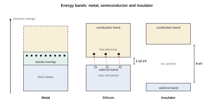
The intrinsic concentration depends steeply on temperature, because the fraction of electrons with enough thermal energy to cross the gap grows exponentially. A useful rule of thumb is that n_i roughly doubles for every 11 °C near room temperature. That single fact explains a great deal of digital behaviour: leakage currents in transistors and diodes are carried by these thermally generated carriers, so leakage climbs steeply as a chip warms up. The NS-4 sits in a sealed metal box on a traffic pole, where summer sun can push the board to 70 °C, so the leakage budget Ines writes for the NS-5 always uses the hot corner, not the 25 °C datasheet line.
Doping: n-type and p-type silicon
Doping replaces a small fraction of silicon atoms with atoms from a neighbouring column of the periodic table. Silicon has four outer electrons. A phosphorus or arsenic atom has five; four bond with neighbours and the fifth is so loosely held that at room temperature it is free. Such atoms are donors, and silicon doped with them is n-type, with electrons as the majority carriers. A boron atom has only three outer electrons, so it leaves a hole in the bonds around it. Boron is an acceptor, and boron-doped silicon is p-type, with holes as the majority carriers.
The doses are small in relative terms but large in effect. Typical doping levels run from 10¹⁵ to 10²⁰ atoms per cubic centimetre, against about 5 × 10²² silicon atoms per cubic centimetre, so even heavy doping replaces only about one atom in five hundred. Yet 10¹⁶ donors per cubic centimetre gives a million times more free electrons than intrinsic silicon. In doped material the product of electron and hole concentrations stays fixed at n_i², which is called the mass-action law. Adding donors therefore suppresses holes: with 10¹⁶ donors, the electron density is about 10¹⁶ and the hole density only about 10⁴ per cubic centimetre.
Carriers move in two ways. Drift is motion under an electric field, with average speed proportional to the field: v = μE, where μ is the mobility. In lightly doped silicon at room temperature electrons have a mobility of about 1,350 cm²/V·s and holes about 480 cm²/V·s. That factor of nearly three between electrons and holes matters throughout this course, because it is why a p-channel transistor must be made wider than an n-channel one to carry the same current. Diffusion is motion from high concentration to low concentration, the same process that spreads a drop of dye in water. Both mechanisms carry current in every device covered here.
The conductivity of a doped region follows directly from the carrier density and mobility, and the resistivity is its inverse. Chip designers use this to make resistors from doped silicon, and it sets the resistance of the channels and contacts in every transistor. It also explains why the polysilicon or metal gate lines in a chip have measurable resistance, which comes back in the lesson on delay.
Worked problem
Resistivity of a doped well
An n-type region is doped with N_D = 10¹⁶ cm⁻³. Take the electron mobility as 1,200 cm²/V·s at this doping and q = 1.602 × 10⁻¹⁹ C. Find the resistivity, and compare it with intrinsic silicon at about 2 × 10⁵ Ω·cm.
Show solution
- \[ \sigma \approx q \, N_D \, \mu_n = 1.602\times10^{-19} \times 10^{16} \times 1200 = 1.92\ \text{S/cm}\]
- \[ \rho = \frac{1}{1.92} \approx 0.52\ \Omega\cdot\text{cm}\]
- \[ \frac{2\times10^{5}}{0.52} \approx 3.8\times10^{5}\]
Answer: The doped region has a resistivity of about 0.52 Ω·cm, roughly 400,000 times lower than intrinsic silicon. The minority holes contribute nothing measurable.
The pn junction
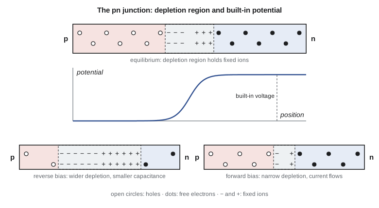
When p-type and n-type regions meet, electrons diffuse from the n side into the p side and holes diffuse the other way. Each carrier that crosses recombines near the boundary and leaves behind a fixed, charged dopant ion: positive donors on the n side and negative acceptors on the p side. These ions form a thin depletion region, empty of free carriers, whose electric field pushes back against further diffusion. Equilibrium is reached when the built-in potential, about 0.6 to 0.8 V for silicon, exactly balances the diffusion tendency.
Applying a voltage changes the balance. A forward bias, positive on the p side, lowers the barrier, and current grows exponentially with voltage, which gives the familiar diode curve with a knee near 0.6 to 0.7 V for silicon at small currents. A reverse bias raises the barrier and widens the depletion region; only a tiny leakage current, carried by thermally generated minority carriers, flows. That leakage is the same thermal effect discussed above, so it roughly doubles every 10 °C. The diode equation summarizes both directions.
Two properties of the junction matter constantly in digital design. First, the depletion region behaves like a capacitor whose plates are the edges of the region; its capacitance falls as reverse bias widens it. Every transistor in a chip has such junctions at its source and drain, and their capacitance is a large part of the load that each gate must charge and discharge. Second, every pn junction is a diode, whether it was meant to be or not. The protection structures on an input pin, the body diodes inside a power MOSFET and the parasitic paths that cause latch-up are all pn junctions behaving exactly as the equation predicts. Lesson 2 uses this directly.
From junctions to transistors
The MOSFET, metal-oxide-semiconductor field-effect transistor, is the device behind nearly all digital logic. In an n-channel MOSFET, two heavily doped n regions, the source and drain, sit in a p-type body. Between them, a thin insulating oxide separates the body surface from a conducting gate. With no gate voltage, the path from source to drain passes through two back-to-back pn junctions and no current flows. A positive gate voltage attracts electrons to the surface under the gate. Once the gate-to-source voltage exceeds the threshold voltage V_t, those electrons form a thin conducting channel, an inversion layer, and current can flow between drain and source. The gate itself draws essentially no steady current, because it is insulated.
A p-channel MOSFET is the mirror image: p-type source and drain in an n-type body, turned on by making the gate negative with respect to the source. CMOS, complementary MOS, places both types on the same chip and wires them so that in every steady state one network of transistors connects the output to the supply or to ground and the other is off. That arrangement draws almost no current except while switching, which is why CMOS took over digital electronics. Lesson 3 builds the MOSFET model, and lessons 4 and 5 assemble it into the inverter and logic gates.
Modern processes add layers to this simple picture. Gate oxides in advanced chips are only a nanometre or two thick, so electrons tunnel through them and create gate leakage; manufacturers replace silicon dioxide with high-permittivity materials to allow a thicker physical layer. Transistors in the most advanced chips are no longer flat: the channel is a vertical fin or a stack of thin sheets wrapped by the gate on several sides, which gives the gate better control and cuts leakage. The microcontrollers on the NS-4 and NS-5 boards use mature, planar processes with feature sizes of tens of nanometres or more, chosen for low leakage and low cost rather than peak speed. The ideas in this course apply to all of them.
Why temperature and process matter
Three variables shape every device in this course: process, voltage and temperature, together called PVT. Process variation means that transistors on different wafers, or even in different places on one chip, come out slightly faster or slower than nominal because of small differences in doping, oxide thickness and dimensions. Voltage variation comes from regulator tolerance, battery state and noise on the supply. Temperature changes mobility, threshold voltage and leakage. Datasheets and chip designers therefore check corners: slow process, low voltage and high temperature for the longest delays, and fast process, high voltage and high temperature for the worst leakage and power.
For a microcontroller user, PVT shows up as ranges in the datasheet: input thresholds as a fraction of the supply rather than fixed voltages, maximum clock frequencies that depend on supply voltage, and leakage and sleep currents quoted at 25 °C and again at 85 or 105 °C. Dev's logbook from last winter shows two NS-4 units that stopped counting at −35 °C during a cold snap. The cause was not the silicon but a crystal oscillator that would not start; the microcontroller itself was specified to −40 °C. The engineering lesson is general: know which part of the system sets each temperature limit.
| Quantity | Rises with temperature? | Effect on digital circuits |
|---|---|---|
| Intrinsic carriers n_i | Yes, steeply (about ×2 per 11 °C) | Junction and channel leakage grow |
| Carrier mobility | No, it falls | On-current falls, gates get slower |
| Threshold voltage | No, it falls (about 1 to 2 mV/°C) | Leakage grows; partly offsets slower mobility |
| Diode forward voltage | No, it falls (about 2 mV/°C) | Clamp and LED voltages shift |
| Wire resistance | Yes (about 0.4 %/°C for copper) | Interconnect delay and IR drop grow |
Simulating carrier density
The code below estimates the intrinsic carrier density of silicon from the band-gap formula, scaled to 1.0 × 10¹⁰ cm⁻³ at 300 K, and shows how fast it grows over the NS-5's operating range. It also computes the ratio between the hottest and coldest cases, which is roughly the ratio by which junction leakage changes.
import math

k = 8.617e-5          # Boltzmann constant in eV/K
Eg = 1.12             # silicon band gap in eV (taken as constant here)
ni_300 = 1.0e10       # intrinsic density at 300 K, cm^-3

def ni(T):
    """Intrinsic carrier density scaled from the 300 K value."""
    return ni_300 * (T / 300) ** 1.5 * math.exp(-Eg / (2 * k) * (1 / T - 1 / 300))

for c in (-40, 0, 25, 70, 85):
    T = c + 273.15
    print(f"{c:4d} C   n_i = {ni(T):9.2e} cm^-3")

ratio = ni(85 + 273.15) / ni(-40 + 273.15)
print(f"n_i ratio, 85 C to -40 C: {ratio:,.0f}")
print(f"doubling interval near 25 C: {11:.0f} C (rule of thumb)")-40 C n_i = 1.37e+07 cm^-3 0 C n_i = 1.03e+09 cm^-3 25 C n_i = 8.66e+09 cm^-3 70 C n_i = 1.86e+11 cm^-3 85 C n_i = 4.39e+11 cm^-3 n_i ratio, 85 C to -40 C: 31,962 doubling interval near 25 C: 11 C (rule of thumb)
The density rises from about 10⁶ at −40 °C to over 10¹¹ at 85 °C, a factor of about a hundred thousand. Leakage that is negligible in a cold enclosure can dominate the sleep current of a hot one. Lesson 7 returns to leakage with real numbers for the NS-5.
Common mistakes
MistakeTreating holes as just the absence of electrons, with no current of their own.
InsteadHoles move and carry current like positive particles, with their own mobility; p-type devices conduct by hole drift.
MistakeAssuming doped silicon is still a poor conductor.
InsteadEven modest doping lowers resistivity by factors of hundreds of thousands; doping sets the conductivity of every region.
MistakeReading leakage and timing from the 25 °C column of a datasheet.
InsteadLeakage is worst hot and timing is worst at the slow, low-voltage, hot corner; design to the corners.
MistakeForgetting that every pn junction is a diode.
InsteadProtection structures, transistor bodies and parasitic paths all behave as diodes and can conduct when biased forward.
Summary and key terms
- Semiconductors have a band gap (1.12 eV for silicon) that thermal energy can bridge for a small fraction of electrons.
- Intrinsic carrier density rises steeply with temperature, so leakage does too.
- Donors make n-type silicon and acceptors make p-type; the product n·p stays equal to n_i².
- Electrons in silicon are about three times more mobile than holes.
- A pn junction forms a depletion region, conducts exponentially when forward biased and leaks slightly when reverse biased.
- Junction depletion regions act as capacitances that every gate must charge.
- A MOSFET uses a gate voltage above threshold to form a conducting channel between source and drain; CMOS pairs n- and p-channel devices.
- Process, voltage and temperature corners set the limits of digital timing, leakage and power.
- Band gap
- The energy range with no electron states between the valence and conduction bands; 1.12 eV in silicon.
- Intrinsic carrier density
- The equal electron and hole density in pure silicon, about 10¹⁰ cm⁻³ at room temperature.
- Donor
- A dopant atom with an extra electron that becomes a free carrier, making n-type material.
- Acceptor
- A dopant atom with one fewer electron that creates a hole, making p-type material.
- Mobility
- The ratio of carrier drift speed to electric field.
- Depletion region
- The carrier-free zone at a pn junction containing fixed dopant ions.
- Threshold voltage
- The gate-to-source voltage at which a MOSFET channel forms.
- PVT corners
- Combinations of process, voltage and temperature extremes used to check worst-case behaviour.
Practice problems
Work each problem on paper first, then reveal the answer to check.
A p-type region has N_A = 10¹⁷ cm⁻³ and n_i = 10¹⁰ cm⁻³. What is the electron density?
Show answer
n = n_i² / N_A = 10²⁰ / 10¹⁷ = 10³ cm⁻³.
Using the rule of thumb, by roughly what factor does n_i grow from 25 °C to 69 °C?
Show answer
44 °C is four doublings, so about 16 times.
Why must a p-channel transistor be wider than an n-channel transistor for equal current?
Show answer
Hole mobility is about one third of electron mobility, so more width is needed to give the same conductance.
What does a reverse-biased pn junction contribute to a digital circuit besides leakage?
Show answer
Capacitance, from its depletion region, which adds to the load that gates must charge.
Lesson quiz · 5 questions
Score 60% or more to complete this lesson.
Create a free account to save your progress, take quizzes and earn a certificate.