
CMP-350 · Lesson 10 of 12 · 23 min
Logic families, voltage levels and level shifting
A real board rarely runs at a single voltage. The NS-5 that Northway Sensing is designing has a 3.3 V microcontroller, a radar module whose data lines run at 5 V, a modem whose interface runs at 1.8 V, and the 12.8 V battery behind all of it. Every connection between two of these domains must pass a logic 0 and a logic 1 reliably, without damaging either side and without wasting power. This lesson surveys the logic families and their voltage thresholds, shows how to test any connection for compatibility, and works through the circuits that translate between levels.
Logic families
Early integrated logic used bipolar transistors. Transistor-transistor logic, TTL, ran from 5 V and became the reference for decades of interface standards: an input reads high above 2.0 V and low below 0.8 V, and an output guarantees at least 2.4 V high and at most 0.4 V low. Those thresholds are asymmetric because of the bipolar input stage, and they survive today in the LVTTL levels of 3.3 V parts. Emitter-coupled logic, ECL, kept its transistors out of saturation for speed, used small swings and drew constant current, and lives on in the differential signalling of high-speed links.
CMOS logic replaced both for almost everything. Its thresholds scale with the supply: a classic 5 V CMOS input reads high above 70 percent of V_DD and low below 30 percent, while its outputs swing nearly to the rails. As supplies fell to 3.3, 2.5, 1.8 and 1.2 V, the JEDEC low-voltage CMOS standards defined thresholds for each, usually as fractions of the supply at the lower voltages. Some CMOS families were built with TTL-compatible inputs, whose thresholds are set near 1.4 V so a 5 V CMOS gate can accept TTL outputs.
| Family | V_OH min | V_OL max | V_IH min | V_IL max |
|---|---|---|---|---|
| 5 V TTL | 2.4 V | 0.4 V | 2.0 V | 0.8 V |
| 5 V CMOS | 4.4 V | 0.5 V | 3.5 V | 1.5 V |
| 3.3 V LVCMOS or LVTTL | 2.9 V | 0.4 V | 2.0 V | 0.8 V |
| 2.5 V LVCMOS | 2.0 V | 0.4 V | 1.7 V | 0.7 V |
| 1.8 V LVCMOS | 1.35 V | 0.45 V | 1.17 V | 0.63 V |
Checking compatibility
A connection works when the driver's guaranteed output levels fall inside the receiver's guaranteed input levels, with margin. That is the noise-margin test from lesson 4 applied between two different parts: the high-level margin is the driver's minimum V_OH minus the receiver's minimum V_IH, and the low-level margin is the receiver's maximum V_IL minus the driver's maximum V_OL. Both must be positive, and comfortably so, after allowing for ground offsets between the parts and for the voltage drop caused by the load current.
A second test is absolute: no input may be driven above its own supply by more than its rating. A 5 V output driving a 3.3 V input easily meets the thresholds, but unless the input is specifically 5 V tolerant, it forces current through the input's clamp diode into the 3.3 V supply, the back-powering problem of lesson 2. Five-volt tolerant pins omit the upper clamp diode and use special protection so they can accept a higher voltage, but often only while the part is powered. Datasheets list these pins separately, and the tolerance can disappear when the pin is configured as an analog input.
Worked problem
The NS-5 radar interface
The radar module's UART uses 5 V CMOS levels. Can the 3.3 V microcontroller's transmit pin drive the radar's receive input directly, and can the radar's transmit pin drive the microcontroller directly?
Show solution
- \[ \text{MCU} \to \text{radar: } NM_H = 2.9 - 3.5 = -0.60\ \text{V}\]
- \[ \text{radar} \to \text{MCU: } NM_H = 4.4 - 2.0 = 2.4\ \text{V}, \qquad NM_L = 0.8 - 0.5 = 0.3\ \text{V}\]
Answer: The microcontroller cannot drive the radar input: its guaranteed high of 2.9 V is 0.6 V short of the 3.5 V the radar needs, so a translator is required in that direction. The radar can drive the microcontroller’s thresholds, with a thin 0.3 V low-level margin, but only if the microcontroller pin is 5 V tolerant; otherwise the 5 V high level must be limited. If the radar had TTL-compatible inputs, the first connection would pass with 0.9 V of high-level margin.
Simple translation: resistors and clamps
For a slow, unidirectional signal going from a higher voltage to a lower one, a resistive divider is the simplest translator. Two resistors scale the 5 V high down to about 3.3 V. The divider's output resistance and the input capacitance form an RC low-pass filter, so the resistors must be small enough for the edge rate: a 10 kΩ and 20 kΩ divider has a Thevenin resistance of 6.7 kΩ, and with 10 pF of input capacitance its time constant is 67 ns, fine for a 115,200 baud UART but not for a 20 MHz SPI clock. The divider also loads the driver continuously while its output is high.
The series-resistor-and-clamp method from lesson 2 is another option for a high-to-low connection: a resistor limits the current that flows through the receiving pin's upper clamp diode to a safe level. It works only if the receiving side's supply can absorb the current, which is not guaranteed when that side is lightly loaded or asleep. For the NS-5, with its sleeping 3.3 V rail, Ines Carvalho rejects that approach because the injected current could hold the sleep supply above its regulation point.
The MOSFET bidirectional shifter
Open-drain buses such as I²C, and single-wire buses, need translation in both directions without a direction signal. The classic solution uses one small n-channel MOSFET per line, with its gate tied to the lower supply, its source on the low-voltage side and its drain on the high-voltage side, and a pull-up resistor on each side to its own supply.
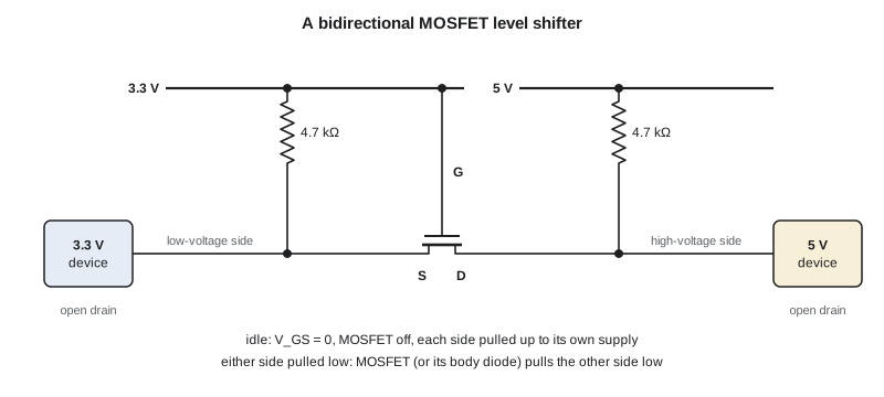
The circuit has three states. When nobody drives the bus, both sides are pulled high to their own supplies; the MOSFET's gate and source are both at 3.3 V, so it is off and isolates the sides. When a device on the low side pulls its line low, the MOSFET's gate-to-source voltage rises to 3.3 V, the transistor turns on and pulls the high side low too. When a device on the high side pulls low, the MOSFET's body diode first pulls the low side down to about 0.6 V, which turns the channel on, and the channel then pulls the low side the rest of the way. The MOSFET must have a threshold voltage well below the low supply, so that it turns on fully with only 3.3 V of gate drive, and a low gate capacitance so it does not slow the edges.
Worked problem
Pull-up resistors for a shifted open-drain bus
The radar module also has a 5 V open-drain configuration bus that Maren Holt's firmware uses at 100 kHz, with a 1,000 ns rise-time limit. The 3.3 V side carries 40 pF and the 5 V side 60 pF. Devices must sink at most 3 mA at 0.4 V. Find the allowed pull-up range on each side, then check 4.7 kΩ on both sides.
Show solution
- \[ R_{\min,3.3} = \frac{3.3 - 0.4}{3\,\text{mA}} = 967\ \Omega, \qquad R_{\min,5} = \frac{5.0 - 0.4}{3\,\text{mA}} = 1{,}533\ \Omega\]
- \[ R_{\max,3.3} = \frac{1000\,\text{ns}}{0.8473 \times 40\,\text{pF}} = 29.5\ \text{k}\Omega, \qquad R_{\max,5} = \frac{1000\,\text{ns}}{0.8473 \times 60\,\text{pF}} = 19.7\ \text{k}\Omega\]
- \[ I_{\text{sink}} = \frac{3.3 - 0.4}{4.7\,\text{k}\Omega} + \frac{5.0 - 0.4}{4.7\,\text{k}\Omega} = 0.62 + 0.98 = 1.60\ \text{mA}\]
Answer: 4.7 kΩ lies inside both ranges. A device on the low side pulling low must sink current from both pull-ups through the MOSFET, 1.60 mA in total, well under its 3 mA limit. The rise times are about 159 ns and 239 ns, comfortably within 1,000 ns, and still within the 300 ns fast-mode limit, which would allow 400 kHz if the radar supports it. The factor 0.8473 comes from the 30 to 70 percent rise time of an RC edge, as used in CMP-315.
The bidirectional MOSFET shifter has limits. Rising edges are passive, set by the pull-ups, so it is slow for push-pull signals above a few megahertz. Each side's pull-up draws current whenever its line is low. And because the gate ties to the low supply, if that supply is off, the MOSFET is off and the sides are isolated, which is usually a feature: a sleeping low-voltage domain is not back-powered by the high side.
Dedicated translators
For fast push-pull signals, dedicated level translator chips are the robust solution. A dual-supply translator powers its A-side buffers from one supply and its B-side buffers from the other, so each side sees clean, full-swing logic for its own voltage. Direction-controlled translators have a pin that selects which way each channel drives; they suit buses such as SPI where every line has a known direction. Auto-direction translators sense which side is driving, which is convenient but can misbehave with strong pull-ups or heavy loads, so their datasheets restrict the load. Most translators include a feature that puts the outputs in high impedance when either supply is absent, which prevents back-powering during power sequencing.
Single-supply buffers with TTL-compatible or over-voltage-tolerant inputs offer a simple one-chip answer for a single direction. A buffer powered from 5 V with TTL thresholds accepts a 3.3 V input and drives a full 5 V output, solving the NS-5 transmit direction. A buffer powered from 3.3 V with over-voltage-tolerant inputs accepts 5 V and drives 3.3 V, solving the receive direction without relying on the microcontroller's pin tolerance.
| Method | Direction | Speed | Notes |
|---|---|---|---|
| Resistive divider | High to low only | Slow; RC limited | Continuous load on driver; cheap |
| Series resistor and clamp | High to low only | Moderate | Injects current into the low supply |
| MOSFET with pull-ups | Bidirectional, open-drain | Up to about 1 MHz | Standard for I²C; no direction pin |
| TTL-input buffer on high supply | Low to high | Fast | Needs a TTL-compatible part |
| Dual-supply translator | Set by pin or automatic | Tens to hundreds of MHz | Best for push-pull buses; handles sequencing |
Differential and low-swing signalling
At high data rates, single-ended rail-to-rail signalling becomes expensive in power and noise. Differential standards such as LVDS send each bit as a small voltage difference, about 350 mV, between two wires driven in opposite directions, with a termination resistor at the receiver. The receiver responds only to the difference, so noise that couples equally onto both wires cancels, and the small swing cuts the CV²f power from lesson 7. Camera and display links, high-speed serial buses and modern memory interfaces all use differential or low-swing signalling, with the translation to logic levels done inside the receiving chip.
Sizing a level shifter with code
The code checks four driver-to-receiver combinations against the guaranteed levels and then sizes the pull-up resistors for a MOSFET shifter in standard and fast modes, confirming the 4.7 kΩ choice.
# Logic-level compatibility and pull-up sizing for a MOSFET level shifter
fam = {   # name: (VOH_min, VOL_max, VIH_min, VIL_max)
    "5 V CMOS":     (4.4, 0.5, 3.5, 1.5),
    "5 V TTL":      (2.4, 0.4, 2.0, 0.8),
    "3.3 V LVCMOS": (2.9, 0.4, 2.0, 0.8),
    "1.8 V LVCMOS": (1.35, 0.45, 1.17, 0.63),
}

def check(drv, rcv):
    voh, vol, _, _ = fam[drv]
    _, _, vih, vil = fam[rcv]
    nmh, nml = voh - vih, vil - vol
    ok = "ok" if nmh > 0 and nml > 0 else "FAILS"
    return f"{drv:13s} -> {rcv:13s} NM_H {nmh:+.2f} V  NM_L {nml:+.2f} V  {ok}"

for d, r in (("3.3 V LVCMOS", "5 V CMOS"), ("3.3 V LVCMOS", "5 V TTL"),
             ("5 V CMOS", "3.3 V LVCMOS"), ("1.8 V LVCMOS", "3.3 V LVCMOS")):
    print(check(d, r))
print("(5 V into a 3.3 V input also needs a 5 V tolerant pin or a translator)")

# open-drain bus through an n-channel MOSFET shifter: 3.3 V side and 5 V side
I_ol, V_ol = 3e-3, 0.4
sides = {"3.3 V side": (3.3, 40e-12), "5 V side": (5.0, 60e-12)}
for mode, t_r in (("standard mode, 1000 ns", 1000e-9), ("fast mode, 300 ns", 300e-9)):
    print(mode)
    for name, (v, c) in sides.items():
        r_min = (v - V_ol) / I_ol
        r_max = t_r / (0.8473 * c)
        print(f"  {name}: R between {r_min:5.0f} and {r_max:6.0f} ohm")

R = 4700
sink = sum((v - V_ol) / R for v, _ in sides.values())
print(f"with 4.7 kOhm on both sides the driver sinks {sink*1e3:.2f} mA when low")
for name, (v, c) in sides.items():
print(f" {name} rise time {0.8473*R*c*1e9:.0f} ns")3.3 V LVCMOS -> 5 V CMOS NM_H -0.60 V NM_L +1.10 V FAILS 3.3 V LVCMOS -> 5 V TTL NM_H +0.90 V NM_L +0.40 V ok 5 V CMOS -> 3.3 V LVCMOS NM_H +2.40 V NM_L +0.30 V ok 1.8 V LVCMOS -> 3.3 V LVCMOS NM_H -0.65 V NM_L +0.35 V FAILS (5 V into a 3.3 V input also needs a 5 V tolerant pin or a translator) standard mode, 1000 ns 3.3 V side: R between 967 and 29505 ohm 5 V side: R between 1533 and 19670 ohm fast mode, 300 ns 3.3 V side: R between 967 and 8852 ohm 5 V side: R between 1533 and 5901 ohm with 4.7 kOhm on both sides the driver sinks 1.60 mA when low 3.3 V side rise time 159 ns 5 V side rise time 239 ns
The output flags the two connections that fail: a 3.3 V output into a 5 V CMOS input, and a 1.8 V output into a 3.3 V input. Both fail on the high-level margin, the usual weak point when driving up to a higher supply. The pull-up results show that the 5 V side, with more capacitance and more voltage to drop, sets the tighter bounds in both modes.
Common mistakes
MistakeChecking only the thresholds when a 5 V signal drives a 3.3 V input.
InsteadUnless the pin is 5 V tolerant, current flows through its clamp diode into the 3.3 V supply.
MistakeAssuming a 3.3 V output can always drive a 5 V input.
InsteadA 5 V CMOS input needs 3.5 V; use a TTL-input buffer or a translator.
MistakeUsing a MOSFET shifter for a fast push-pull bus.
InsteadIts rising edges depend on pull-ups; use a dual-supply translator for fast signals.
MistakeIgnoring power sequencing.
InsteadChoose translators that isolate both sides when either supply is off.
Summary and key terms
- TTL thresholds of 2.0 V and 0.8 V persist in 3.3 V LVTTL and TTL-compatible CMOS inputs.
- CMOS thresholds scale with the supply; JEDEC defines levels for 3.3, 2.5, 1.8 and 1.2 V.
- A connection needs positive high and low noise margins between driver and receiver.
- A higher-voltage signal into a lower-voltage pin needs a tolerant pin or limiting.
- Resistive dividers suit slow, high-to-low signals; their RC limits speed.
- The MOSFET shifter translates open-drain buses in both directions with a pull-up on each side.
- Dual-supply translators handle fast push-pull buses and supply sequencing.
- Differential low-swing signalling saves power and rejects common-mode noise.
- TTL levels
- Input thresholds of 2.0 V high and 0.8 V low, inherited from bipolar logic.
- LVCMOS
- Low-voltage CMOS interface standards for supplies of 3.3 V and below.
- Five-volt tolerant
- A pin that accepts 5 V inputs while powered from a lower supply.
- Level translator
- A circuit that passes logic signals between two voltage domains.
- Bidirectional shifter
- A translator that passes signals either way without a direction control.
- Dual-supply translator
- A buffer chip with each side powered from its own supply.
- Back-powering
- Unintended powering of a domain through its input clamp diodes.
- LVDS
- Low-voltage differential signalling with about 350 mV of swing.
Practice problems
Work each problem on paper first, then reveal the answer to check.
A 2.5 V output with V_OH min 2.0 V drives a 3.3 V LVCMOS input. What is the high-level margin?
Show answer
2.0 − 2.0 = 0 V, unacceptable; use a translator.
A 5 V to 3.3 V divider uses 2.2 kΩ and 3.3 kΩ. What is the output high level, and its source resistance?
Show answer
5 × 3.3 ÷ 5.5 = 3.0 V; 2.2 ∥ 3.3 = 1.32 kΩ.
An open-drain line at 3.3 V has 100 pF and a 300 ns rise limit. What is the largest pull-up?
Show answer
300 ns ÷ (0.8473 × 100 pF) ≈ 3.5 kΩ.
Why must the MOSFET in a bidirectional shifter have a low threshold voltage?
Show answer
Its gate drive is only the low supply voltage, so it must turn fully on with, for example, 3.3 V or 1.8 V.
Lesson quiz · 5 questions
Score 60% or more to complete this lesson.
Create a free account to save your progress, take quizzes and earn a certificate.