
CMP-350 · Lesson 3 of 12 · 19 min
The MOSFET as a switch: operation and models
A digital chip is billions of switches, and the switch is the MOSFET. Lesson 1 described how a gate voltage above threshold forms a channel between source and drain. This lesson turns that picture into models a designer can calculate with: the regions of operation, the square-law current equation, the on-resistance a switch presents, the capacitances that every gate drives, and the short-channel effects that change the picture in modern processes. ELE-240 uses the same device as an amplifier and focuses on small-signal behaviour around a bias point. Here the interest is in the two ends of the range, fully on and fully off, and in how quickly the transistor moves between them.
Structure and symbols
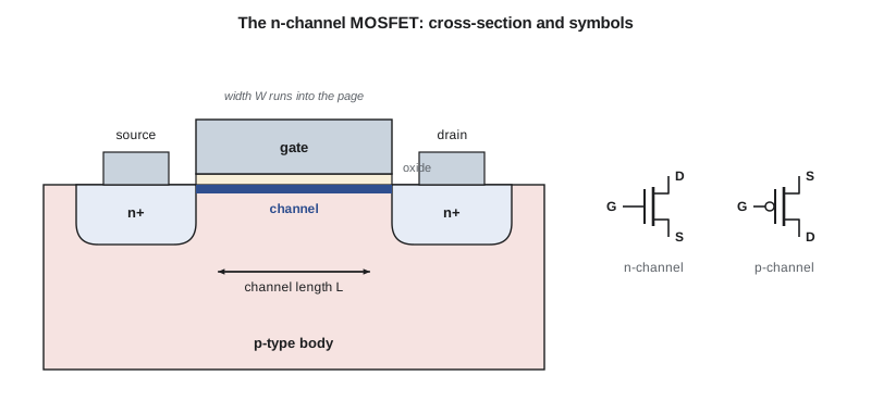
An n-channel MOSFET has four terminals: gate, source, drain and body (also called the bulk or substrate). In a digital chip the body of every n-channel device is tied to ground and the body of every p-channel device to the supply, so circuit diagrams usually show only three terminals. The source is whichever end of the channel has the lower voltage in an n-channel device, or the higher voltage in a p-channel device; the structure is symmetric, so the roles can swap during operation, as they do in the pass transistors of an SRAM cell in lesson 9. The key dimensions are the channel length L, the distance from source to drain under the gate, and the channel width W, measured across. The ratio W/L sets how much current the transistor can carry.
Regions of operation
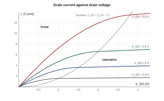
For an n-channel device, three regions describe the long-channel behaviour. In cutoff, V_GS is below the threshold V_t and almost no current flows; there is no channel. In the linear region, also called the triode region, V_GS exceeds V_t and the drain-to-source voltage V_DS is small, so the channel stretches the whole way from source to drain and the device acts like a resistor whose value is controlled by the gate. In saturation, V_DS has grown beyond V_GS − V_t, the channel pinches off near the drain, and the current stops growing with V_DS; the device acts like a current source controlled by the gate. The quantity V_GS − V_t, called the overdrive voltage V_ov, appears in every equation.
The process transconductance parameter k_n equals the electron mobility times the gate oxide capacitance per unit area, μ_n C_ox. It is fixed by the manufacturing process. A designer controls W and L. For p-channel devices the same equations apply with all voltages and the current reversed in sign and with the hole mobility, so k_p is roughly a third to a half of k_n. That is why the pull-up transistors in a CMOS gate are drawn wider than the pull-downs: a p-channel device with twice or three times the width of an n-channel device gives about the same current.
The MOSFET as a switch: on-resistance
When a MOSFET is used as a switch, it is driven hard on with V_GS well above V_t and carries current with only a small V_DS across it. Deep in the linear region the V_DS² term is negligible, and the device looks like a resistor. That on-resistance sets how fast a gate can charge a load and how much power a load switch wastes. It falls as the gate drive rises, which is one reason chips slow down when the supply voltage drops.
The same equation explains discrete power MOSFETs, which reach on-resistances of a few milliohms by connecting thousands of small transistor cells in parallel to make an enormous effective width. Their datasheets give R_DS(on) at specific gate voltages, such as 4.5 V and 10 V, and often a much higher value at 2.5 V. A logic-level MOSFET is one specified to turn on fully at the gate voltage a microcontroller can supply; choosing a power MOSFET rated only at 10 V and driving it from a 3.3 V pin is a classic mistake that leaves the device half on and hot. Lesson 11 makes this concrete.
Worked problem
On-resistance of an output transistor
An n-channel output transistor in a 3.3 V microcontroller pin has k_n = 300 µA/V², W/L = 400 and V_t = 0.5 V. With the gate at 3.3 V, estimate its on-resistance, and the output voltage when it sinks 8 mA.
Show solution
- \[ V_{ov} = 3.3 - 0.5 = 2.8\ \text{V}\]
- \[ R_{\text{on}} \approx \frac{1}{300\times10^{-6} \times 400 \times 2.8} = \frac{1}{0.336} \approx 2.98\ \Omega\]
- \[ V_{OL} \approx 8\ \text{mA} \times 2.98\ \Omega \approx 24\ \text{mV}\]
Answer: This simple model predicts about 3 Ω and a 24 mV drop. Real datasheets quote V_OL of 0.4 V at 8 mA or more because short-channel effects, explained below, and process and temperature corners raise the effective resistance. The model is a starting point, not a substitute for the datasheet.
Capacitances: what every gate must charge
A MOSFET's speed in a digital circuit is limited less by the transistor itself than by the capacitance it must charge and discharge. The gate is one plate of a capacitor with the channel as the other, separated by the oxide, so the gate capacitance is roughly C_ox times W times L. There are also overlap capacitances where the gate extends slightly over the source and drain, and junction capacitances where the source and drain regions meet the body, as lesson 1 described. Interconnect wires add their own capacitance to ground and to neighbouring wires. When a gate drives another gate, the load is the input capacitance of the next gate plus the wire plus the drain junctions of its own output transistors.
Because current rises with W but so does capacitance, making a transistor wider does not make a circuit faster without limit: a wider transistor drives its load faster but presents a bigger load to whatever drives it. Lesson 5 turns this trade-off into the method of logical effort, and lesson 6 into delay estimates. For now the key point is that a digital gate is an RC circuit: a resistance set by the on-transistors charging a capacitance set by everything connected to the output.
Below threshold: subthreshold conduction
The cutoff region is not truly off. Below threshold, a small current still flows by diffusion of carriers that have enough thermal energy to cross the barrier, and it falls exponentially as V_GS drops. The subthreshold slope, the change in gate voltage for a factor of ten change in current, is at best about 60 mV per decade at room temperature and is typically 70 to 100 mV per decade in real devices. A transistor with V_t = 0.5 V and a slope of 80 mV per decade therefore carries roughly 10^(500/80), about 1.8 million, times less current at V_GS = 0 than at threshold. That leftover current, summed over millions of transistors, is the leakage that dominates the sleep current of a large chip.
Lowering V_t makes a transistor faster, because the overdrive at a given supply is larger, but every 80 mV of reduction multiplies the off-current by ten. Chip designers handle this with several transistor types on one chip: low-threshold devices on critical speed paths and high-threshold devices elsewhere. Microcontrollers aimed at battery products, like those on the NS-4 and NS-5, use high-threshold, low-leakage processes and accept a lower maximum clock rate in exchange. Lesson 7 puts numbers on the trade.
Short-channel effects
The square law describes long-channel devices well. In modern transistors, with channel lengths of tens of nanometres, several effects bend the picture. Velocity saturation is the most important: in a very short channel the electric field is so high that carriers reach a maximum drift speed, around 10⁷ cm/s for electrons, and current then grows roughly linearly with overdrive rather than with its square. Channel-length modulation makes the saturation current rise slowly with V_DS, because the pinch-off point moves toward the source and the effective channel shortens. Drain-induced barrier lowering lets a high drain voltage reduce the threshold, which increases leakage. The practical result is captured by the alpha-power law, in which current rises as overdrive to a power between 1 and 2.
| Effect | Cause | Consequence for digital circuits |
|---|---|---|
| Velocity saturation | High lateral field in short channels | Current grows more slowly with gate voltage; α nearer 1 |
| Channel-length modulation | Pinch-off point moves with V_DS | Saturation current rises slightly with V_DS |
| Drain-induced barrier lowering | Drain field reaches the source barrier | Threshold falls at high V_DS; leakage rises |
| Gate tunnelling | Very thin gate oxide | Gate leakage current; high-permittivity dielectrics used |
| Threshold variation | Few dopant atoms in a tiny channel | Mismatch between neighbouring transistors; SRAM margins shrink |
Simulating the square law
The code below uses the long-channel model to compute drain current for an n-channel transistor across its regions, its on-resistance as gate drive changes, and the effect of the supply on switching current. It also compares a square-law and an alpha-power estimate of how saturation current changes when the supply drops from 3.3 V to 1.8 V, which is the kind of question Ines asks when deciding whether the NS-5 can run its logic at a lower voltage.
kn = 300e-6      # A/V^2, process parameter
WL = 20          # width-to-length ratio
Vt = 0.5         # threshold voltage, V

def drain_current(vgs, vds):
    vov = vgs - Vt
    if vov <= 0:
        return 0.0
    if vds < vov:                                   # linear region
        return kn * WL * (vov * vds - 0.5 * vds ** 2)
    return 0.5 * kn * WL * vov ** 2                 # saturation

print("Vgs   Vds   Id (mA)  region")
for vgs, vds in [(0.3, 1.0), (1.5, 0.2), (1.5, 2.0), (3.3, 0.2), (3.3, 3.3)]:
    vov = vgs - Vt
    region = "cutoff" if vov <= 0 else ("linear" if vds < vov else "saturation")
    print(f"{vgs:3.1f}  {vds:4.1f}  {drain_current(vgs, vds) * 1e3:7.3f}  {region}")

print("\nOn-resistance versus gate drive (W/L = 20)")
for vgs in (1.2, 1.8, 2.5, 3.3):
    ron = 1 / (kn * WL * (vgs - Vt))
    print(f"Vgs = {vgs:.1f} V  Ron = {ron:6.1f} ohm")

def ratio(v1, v2, alpha):
    return ((v2 - Vt) / (v1 - Vt)) ** alpha

print("\nSaturation current at 1.8 V relative to 3.3 V")
print(f"square law (alpha = 2):   {ratio(3.3, 1.8, 2.0):.2f}")
print(f"short channel (alpha = 1.3): {ratio(3.3, 1.8, 1.3):.2f}")Vgs Vds Id (mA) region 0.3 1.0 0.000 cutoff 1.5 0.2 1.080 linear 1.5 2.0 3.000 saturation 3.3 0.2 3.240 linear 3.3 3.3 23.520 saturation On-resistance versus gate drive (W/L = 20) Vgs = 1.2 V Ron = 238.1 ohm Vgs = 1.8 V Ron = 128.2 ohm Vgs = 2.5 V Ron = 83.3 ohm Vgs = 3.3 V Ron = 59.5 ohm Saturation current at 1.8 V relative to 3.3 V square law (alpha = 2): 0.22 short channel (alpha = 1.3): 0.37
Dropping the supply from 3.3 V to 1.8 V cuts the overdrive from 2.8 V to 1.3 V. With the square law the current falls to about 22 percent; with α = 1.3 it falls to about 37 percent. Either way the gates get noticeably slower, which is why a microcontroller's maximum clock frequency is specified against supply voltage. Lesson 7 shows that the energy saved per operation can still make the lower voltage worthwhile.
Common mistakes
MistakeAssuming a MOSFET in cutoff draws zero current.
InsteadSubthreshold conduction falls exponentially but never reaches zero; summed over a chip it is the leakage current.
MistakeDriving a power MOSFET rated only at 10 V gate drive from a 3.3 V pin.
InsteadChoose a logic-level MOSFET with R_DS(on) specified at the available gate voltage.
MistakeUsing the square law for modern short-channel devices without question.
InsteadVelocity saturation makes current grow closer to linearly with overdrive; use measured data or an alpha-power fit.
MistakeMaking transistors wider to make a circuit faster without limit.
InsteadA wider transistor drives more current but presents more capacitance to its driver; size by logical effort.
Summary and key terms
- A MOSFET has cutoff, linear and saturation regions defined by V_GS − V_t and V_DS.
- In the linear region it acts as a gate-controlled resistor; in saturation, a gate-controlled current source.
- Current scales with W/L and with k = μC_ox; p-channel devices need more width for the same current.
- On-resistance falls as gate drive rises; logic-level power MOSFETs are specified at low gate voltages.
- Gate, overlap, junction and wire capacitances make every gate an RC circuit.
- Subthreshold current falls by ten for every 60 to 100 mV below threshold; it sets leakage.
- Short-channel effects such as velocity saturation weaken the square law in modern devices.
- Threshold voltage
- The gate-to-source voltage at which the channel forms.
- Overdrive voltage
- V_GS minus V_t; the gate voltage available to drive current.
- Linear (triode) region
- Operation with small V_DS, where the device behaves as a resistor.
- Saturation region
- Operation with V_DS above the overdrive, where current is nearly independent of V_DS.
- On-resistance
- The drain-to-source resistance of a fully on transistor.
- Subthreshold slope
- The gate-voltage change per decade of current below threshold.
- Velocity saturation
- The limit on carrier speed at high fields, which makes current grow more slowly with gate voltage.
- Logic-level MOSFET
- A power MOSFET specified to turn fully on at gate voltages a logic circuit can supply.
Practice problems
Work each problem on paper first, then reveal the answer to check.
An n-channel device has k_n = 200 µA/V², W/L = 10, V_t = 0.6 V and V_GS = 1.8 V. What is its saturation current?
Show answer
½ × 200 µA × 10 × 1.2² = 1.44 mA.
With S = 90 mV per decade, by what factor does subthreshold current fall when V_GS drops by 270 mV?
Show answer
10^(270/90) = 1,000.
Why does a chip's maximum clock frequency fall at lower supply voltage?
Show answer
Lower overdrive gives less current, so gates charge their loads more slowly.
What is the on-resistance of a switch with k_n = 300 µA/V², W/L = 100 and V_ov = 1.5 V?
Show answer
1 / (300 µA × 100 × 1.5) ≈ 22 Ω.
Lesson quiz · 5 questions
Score 60% or more to complete this lesson.
Create a free account to save your progress, take quizzes and earn a certificate.