
CMP-350 · Lesson 12 of 12 · 25 min
Signal integrity and power delivery
Up to this point, wires have been resistances and capacitances and supplies have been ideal. On a real board, fast edges travel as waves along traces and reflect from their ends, neighbouring traces couple into each other, and the current that every gate draws from its supply must flow through inductance that resists sudden change. Signal integrity is the discipline of keeping logic waveforms clean enough to meet the noise margins of lesson 4; power integrity is the discipline of keeping supply voltages steady while loads change. This closing lesson applies both to the NS-5 board and brings together delay, power and interfacing from the rest of the course.
When a trace becomes a transmission line
An edge travels along a trace on a typical glass-epoxy board at roughly half the speed of light, about 6 to 7 ps per millimetre for a trace inside the board. If the trace is short compared with the distance an edge covers during its own rise time, the whole trace charges almost uniformly and the lumped RC model of lesson 6 is adequate. If it is long, the far end sees the edge later than the near end, and waves reflecting from mismatched ends add to the signal. A common rule treats a trace as a transmission line once its one-way delay exceeds about one sixth of the rise time.
The rise time, not the clock frequency, is what matters. A 1 MHz signal with 1 ns edges needs the same care as a 100 MHz signal with 1 ns edges. With 6.7 ps per millimetre, a 5 ns edge allows about 12 cm of trace before line effects matter, a 1 ns edge about 2.5 cm and a 0.3 ns edge only about 7 mm. The NS-5 microcontroller pin at high drive produces edges of about 1.1 ns, as lesson 6 calculated, so the 8 cm trace to the radar module is well beyond the critical length and must be treated as a line.
| Rise time | Critical length (6.7 ps/mm) | Typical source |
|---|---|---|
| 5 ns | About 12 cm | Slow GPIO drive setting, older logic |
| 1 ns | About 2.5 cm | Microcontroller pin at high drive |
| 0.3 ns | About 7 mm | Fast logic, memory interfaces |
| 0.05 ns | About 1 mm | Multi-gigabit serial links |
Characteristic impedance and reflections
A transmission line has a characteristic impedance Z_0, the ratio of voltage to current for a wave travelling along it, set by the trace width, the dielectric thickness and its permittivity. Typical single-ended board traces are designed for 50 Ω. When a wave reaches a load whose impedance differs from Z_0, part of it reflects, with a reflection coefficient Γ that runs from −1 for a short circuit through 0 for a matched load to +1 for an open circuit.
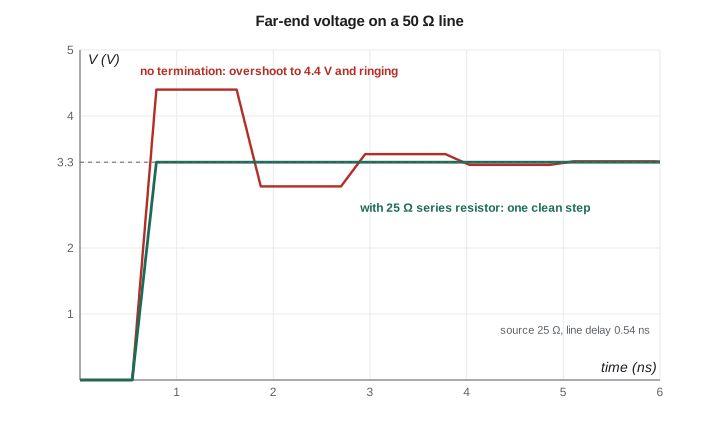
A CMOS input looks like an open circuit with a few picofarads, so Γ is close to +1 at the far end, and the incoming wave doubles. The reflected wave travels back to the driver, whose output resistance is usually lower than Z_0, so it reflects again with negative Γ, and the far end rings above and below the final level. Ringing that crosses the input thresholds produces false edges, which on a clock or a strobe line means extra clock pulses, and overshoot beyond the supply drives current into clamp diodes.
Worked problem
Terminating the radar data line
The 8 cm trace from the NS-5 microcontroller to the radar module has Z_0 = 50 Ω. The microcontroller pin at high drive has an output resistance of about 25 Ω. Find the far-end voltage of the first wave without termination, and the series resistor that removes the ringing.
Show solution
- \[ V_{\text{launch}} = 3.3 \times \frac{50}{50 + 25} = 2.20\ \text{V}, \qquad \Gamma_{\text{far}} \approx +1\]
- \[ V_{\text{far}} = 2 \times 2.20 = 4.40\ \text{V}, \qquad \Gamma_{\text{source}} = \frac{25 - 50}{25 + 50} = -0.33\]
- \[ R_{\text{series}} = Z_0 - R_s = 50 - 25 = 25\ \Omega \;\to\; V_{\text{launch}} = 1.65\ \text{V},\ V_{\text{far}} = 3.30\ \text{V}\]
Answer: Without termination the far end overshoots to about 4.4 V, a volt above the supply, and then rings as the reflections bounce. A 25 Ω series resistor at the driver, a standard value of 22 Ω in practice, matches the source to the line: the launched wave is half the swing, it doubles at the open far end to exactly 3.3 V, and the reflection is absorbed when it returns to the matched source. Selecting the pin’s lower drive strength, which slows the edge beyond the critical length, is the other remedy.
Series termination is the usual choice for point-to-point connections because it costs one resistor and no static power. Its limitation is that the voltage along the line sits at half swing until the reflection returns, so loads in the middle of the line see a staircase; it is wrong for buses with several receivers along their length. Parallel termination, a resistor equal to Z_0 at the far end, absorbs the wave on arrival and suits multi-drop lines, but it draws static current. Differential links such as LVDS from lesson 10 use a 100 Ω resistor across the pair at the receiver.
Crosstalk and return paths
Every signal current returns to its source, and at high frequency the return current flows in the reference plane directly beneath the trace, because that path has the lowest inductance. A solid ground plane under every fast trace keeps the loop small, controls the impedance and minimizes both radiation and susceptibility. A slot or split in the plane forces the return current to detour around it, enlarging the loop, raising inductance and turning the trace into an antenna. Changing layers through a via without a nearby ground via for the return current has the same effect.
Neighbouring traces couple through mutual capacitance and mutual inductance. A fast edge on an aggressor trace induces a pulse on a quiet victim trace, crosstalk, whose size grows with the parallel length and falls quickly with spacing. The usual rule of thumb keeps fast traces at least three trace widths apart, keeps clocks away from sensitive analog lines such as the radar's analog output, and routes them over an unbroken plane.
Ground bounce
The ground and supply connections of a chip pass through package pins, bond wires and vias, each with an inductance of about 1 nH. When several outputs switch at once, their combined current changes quickly through that shared inductance and the chip's internal ground moves relative to the board ground by L di/dt. To the chip's inputs, that movement looks like noise on every signal referenced to the board.
If eight outputs each switch 10 mA in 2 ns through 2 nH of shared ground inductance, the bounce is 2 nH × 80 mA ÷ 2 ns = 80 mV. That is small against a 1.65 V margin but not negligible on a 1.2 V core or on an analog reference. Remedies are the same as for crosstalk: slower edges where speed is not needed, several ground and supply pins, short connections into the planes, and spreading out the outputs that switch together.
Power delivery and decoupling
A regulator holds its output steady only for changes slower than its control loop, typically tens of kilohertz to a few hundred kilohertz. Faster current steps must be supplied from charge stored in capacitors near the load until the regulator catches up. The basic sizing comes from the charge the capacitor must supply: a current step I lasting Δt, with an allowed droop ΔV, needs a capacitance of IΔt/ΔV. Power-integrity engineers often express the same requirement as a target impedance, the allowed droop divided by the current step, which the supply network must stay below at every frequency up to the load's edge rate.
Worked problem
Sizing the modem bulk capacitor
When the NS-5 modem begins a transmit burst, its current jumps to 0.45 A. The regulator feeding the modem rail takes about 20 µs to respond, and the rail may droop by no more than 0.1 V. Size the bulk capacitance, find the target impedance, and explain why the capacitor cannot supply the whole 40 ms burst.
Show solution
- \[ C \ge \frac{0.45\,\text{A} \times 20\,\mu\text{s}}{0.1\,\text{V}} = 90\ \mu\text{F} \;\to\; 100\ \mu\text{F}\]
- \[ Z_{\text{target}} = \frac{0.1\,\text{V}}{0.45\,\text{A}} = 0.22\ \Omega\]
- \[ C_{\text{whole burst}} = \frac{0.45\,\text{A} \times 40\,\text{ms}}{0.1\,\text{V}} = 0.18\ \text{F}\]
Answer: A 100 µF capacitor, the value that lesson 11’s load switch soft-starts, covers the 20 µs until the regulator responds. Its equivalent series resistance must also be well under 0.22 Ω, or the instant drop across the resistance alone uses up the budget, which favours ceramic or polymer capacitors over older electrolytic types. Supplying the whole 40 ms burst from the capacitor would need 0.18 F, a supercapacitor; that is the regulator’s job, and in turn the battery’s, whose internal resistance at cold temperature CMP-315 included in the budget.
Higher-frequency current steps come from the logic itself: every clock edge in the microcontroller core draws a spike of current lasting nanoseconds. Those spikes are supplied first by capacitance on the die and in the package, then by small ceramic capacitors placed right at the supply pins. A step of 5 mA for 10 ns with 50 mV of allowed droop needs only 1 nF, but the capacitor must be able to deliver it quickly, which is limited by inductance rather than capacitance.
Real capacitors: ESR, ESL and resonance
A real capacitor is a capacitance in series with an equivalent series resistance and an equivalent series inductance, the latter set largely by its package size and its mounting: the pads, traces and vias that connect it to the planes. Its impedance falls with frequency like a capacitor until it reaches its self-resonant frequency, where the capacitance and inductance cancel and only the ESR remains, and above that it rises like an inductor. A 100 nF capacitor with 1 nH of mounted inductance resonates near 16 MHz; above that, adding more capacitance of the same kind does not help, but lowering the inductance does.
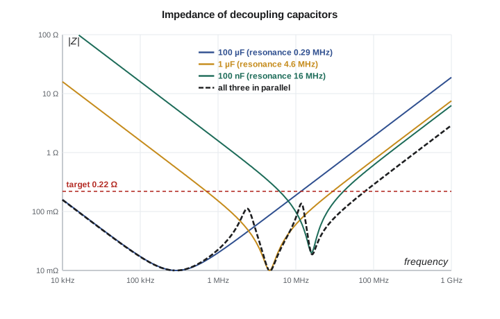
That behaviour explains the standard decoupling pattern. A bulk capacitor of tens to hundreds of microfarads covers the low frequencies up to the regulator’s weakness; a few 1 µF ceramics cover the middle; and a 100 nF or smaller ceramic at each supply pin, mounted with the shortest possible connection to the planes, covers the high frequencies up to where the package and die capacitance take over. The capacitors must be placed so that the current loop from the pin through the capacitor to the ground pin is as small as possible: a via right at each pad and a capacitor on the same side of the board as the chip, within a few millimetres of its pins.
| Stage | Typical parts | Frequency range served | What limits it |
|---|---|---|---|
| Regulator | Linear or switching regulator | DC to about 100 kHz | Control loop bandwidth |
| Bulk | 10 to 470 µF polymer or ceramic | About 1 to 500 kHz | ESR and ESL |
| Mid-frequency | 1 to 10 µF ceramic | About 100 kHz to 10 MHz | Mounting inductance |
| Local | 10 to 100 nF ceramic at each pin | About 5 to 100 MHz | Pad and via inductance |
| Package and die | On-package and on-die capacitance | Above about 100 MHz | Die area |
Putting it together on the NS-5
The final layout review for the NS-5 brings in every lesson of the course. The radar data line gets a 22 Ω series resistor and a solid plane beneath it. The level translator from lesson 10 sits close to the radar connector, with its own 100 nF capacitors on both supplies. The valve driver's flyback diode from lesson 11 sits right at the connector so the kickback loop stays short and away from the microcontroller. The modem's load switch and 100 µF bulk capacitor sit next to the modem, with a wide trace back to the regulator. The microcontroller gets a 100 nF capacitor at each supply pin and a 1 µF capacitor nearby, and its unused pins are configured as outputs or with pulls so they neither float nor draw shoot-through current, as lesson 4 explained. Jonah Abara's final checklist uses the same calculations as the examples of this lesson.
Computing signal and power integrity with code
The code computes critical lengths for three rise times, the reflection and series termination of the radar line, the decoupling capacitance for the modem and the microcontroller, the self-resonance of three capacitors and the ground bounce of eight switching outputs.
# Signal integrity and power delivery: reflections, termination and decoupling
import math

# when is a trace a transmission line? delay about 6.7 ps/mm inside the board
t_pd = 6.7e-12
for t_r in (5e-9, 1e-9, 0.3e-9):
    crit = t_r / (6 * t_pd) * 1e-3          # common rule: line delay above t_r / 6
    print(f"rise time {t_r*1e9:.1f} ns: treat traces longer than about {crit*100:.1f} cm as lines")

# reflections at the far end of a 50 ohm line driven by a 25 ohm source
Z0, Rs = 50.0, 25.0
gamma = lambda zl: (zl - Z0) / (zl + Z0)
print(f"open end gamma {gamma(1e12):+.2f}, source gamma {gamma(Rs):+.2f}")
v_launch = 3.3 * Z0 / (Z0 + Rs)
print(f"unterminated: launch {v_launch:.2f} V, far end first peak {v_launch*2:.2f} V")
R_series = Z0 - Rs
print(f"series termination {R_series:.0f} ohm: launch {3.3*Z0/(Z0+Rs+R_series):.2f} V, far end {3.3:.2f} V")

# decoupling capacitance: C = I * dt / dV
def c_needed(i, dt, dv):
    return i * dt / dv
print(f"modem step 0.45 A for 20 us, 0.1 V droop: {c_needed(0.45, 20e-6, 0.1)*1e6:.0f} uF")
print(f"whole 40 ms burst from the capacitor alone: {c_needed(0.45, 40e-3, 0.1)*1e3:.0f} mF")
print(f"MCU core step 5 mA for 10 ns, 50 mV droop: {c_needed(5e-3, 10e-9, 0.05)*1e9:.1f} nF")
print(f"target impedance for the modem rail: {0.1/0.45*1e3:.0f} mOhm")

# a real capacitor: series resonance of C with its mounting inductance
for c, esl in ((100e-9, 1.0e-9), (1e-6, 1.2e-9), (100e-6, 3e-9)):
    f0 = 1 / (2 * math.pi * math.sqrt(esl * c))
    print(f"{c*1e6:7g} uF with {esl*1e9:.1f} nH: self-resonance {f0/1e6:7.2f} MHz")

# ground bounce: eight outputs switching 10 mA in 2 ns through 2 nH of shared ground
L, di, dt = 2e-9, 8 * 10e-3, 2e-9
print(f"ground bounce about {L*di/dt*1e3:.0f} mV")rise time 5.0 ns: treat traces longer than about 12.4 cm as lines
rise time 1.0 ns: treat traces longer than about 2.5 cm as lines
rise time 0.3 ns: treat traces longer than about 0.7 cm as lines
open end gamma +1.00, source gamma -0.33
unterminated: launch 2.20 V, far end first peak 4.40 V
series termination 25 ohm: launch 1.65 V, far end 3.30 V
modem step 0.45 A for 20 us, 0.1 V droop: 90 uF
whole 40 ms burst from the capacitor alone: 180 mF
MCU core step 5 mA for 10 ns, 50 mV droop: 1.0 nF
target impedance for the modem rail: 222 mOhm
0.1 uF with 1.0 nH: self-resonance 15.92 MHz
1 uF with 1.2 nH: self-resonance 4.59 MHz
100 uF with 3.0 nH: self-resonance 0.29 MHz
ground bounce about 80 mVEach number in the output appears in the lesson. Together they show why the course ends here: the transistors and gates of the earlier lessons are fast and efficient only if the board delivers their signals and supply current cleanly, and the calculations that ensure it are short enough to do by hand or with a few lines of code.
Common mistakes
MistakeJudging whether a trace is a transmission line from the clock frequency.
InsteadThe rise time sets the critical length; slow clocks with fast edges still ring.
MistakeUsing series termination on a multi-drop bus.
InsteadReceivers in the middle see a half-swing step; use parallel termination or a point-to-point topology.
MistakeRouting a fast trace across a split in the ground plane.
InsteadThe return current detours, enlarging the loop; keep an unbroken plane beneath fast signals.
MistakeAdding more 100 nF capacitors to fix noise above their self-resonance.
InsteadAt high frequency, inductance dominates; shorten the mounting or use smaller packages.
MistakeTrying to supply a long load burst from a decoupling capacitor.
InsteadCapacitors bridge the regulator’s response time; the regulator and source supply the rest.
Summary and key terms
- A trace behaves as a transmission line when its delay exceeds about one sixth of the rise time.
- Reflections follow Γ = (Z_L − Z_0)/(Z_L + Z_0); an unterminated CMOS input reflects almost fully.
- Series termination matches the source to the line for point-to-point links.
- Return currents flow beneath the trace; keep ground planes unbroken under fast signals.
- Crosstalk grows with parallel length and falls with spacing.
- Ground bounce is L di/dt through shared package and via inductance.
- Decoupling capacitance must satisfy C ≥ IΔt/ΔV and keep the supply below its target impedance.
- Capacitors resonate with their mounting inductance; a hierarchy of values covers the frequency range.
- Transmission line
- A trace long enough that waves and reflections along it must be considered.
- Characteristic impedance
- The voltage-to-current ratio of a wave travelling along a line.
- Reflection coefficient
- The fraction of an incident wave reflected at an impedance change.
- Series termination
- A resistor at the driver that brings its output resistance up to Z_0.
- Crosstalk
- Unwanted coupling of a signal from one trace onto a neighbouring trace.
- Ground bounce
- Movement of a chip’s internal ground caused by fast current changes through inductance.
- Target impedance
- The highest supply-network impedance that keeps droop within limits.
- Self-resonant frequency
- The frequency at which a capacitor’s capacitance and series inductance cancel.
Practice problems
Work each problem on paper first, then reveal the answer to check.
A signal has 2 ns edges on a board with 6.7 ps/mm. What is the critical length?
Show answer
2 ns ÷ (6 × 6.7 ps/mm) ≈ 50 mm.
A 75 Ω load terminates a 50 Ω line. What is the reflection coefficient?
Show answer
(75 − 50) ÷ 125 = +0.2.
A load steps by 1 A for 5 µs with 50 mV allowed droop. What capacitance is needed?
Show answer
1 A × 5 µs ÷ 0.05 V = 100 µF.
A 10 nF capacitor has 0.8 nH of mounted inductance. What is its self-resonant frequency?
Show answer
1 ÷ (2π √(0.8 nH × 10 nF)) ≈ 56 MHz.
Lesson quiz · 5 questions
Score 60% or more to complete this lesson.
Create a free account to save your progress, take quizzes and earn a certificate.