
CINE-201 · Lesson 2 of 12 · 25 min
How image sensors work
The image sensor is where light becomes data. Every characteristic that cinematographers care about, including sensitivity, noise, dynamic range, colour and the way highlights and shadows behave, begins with the physics of the sensor. Modern sensors are remarkable devices: tens of millions of photosites, each a few micrometres across, that count photons with high efficiency and convert them into numbers thousands of times per second. This lesson explains how a photosite works, the measures that describe it, how charge is read out and digitized, the difference between CMOS and CCD sensors, and the design features, such as microlenses, back-side illumination and stacked construction, that have improved sensors over the past two decades.
The photoelectric effect and the photosite
Image sensors are built on silicon. When a photon of visible light strikes silicon, it can transfer its energy to an electron, freeing it from its atom; this is the photoelectric effect. Each photosite contains a photodiode, a region of silicon with an electric field that collects these freed electrons and holds them during the exposure. The more light falls on the photosite, the more electrons accumulate, so the charge at the end of the exposure is proportional to the light received. At the end of the exposure, the charge is measured and the photosite is reset for the next frame.
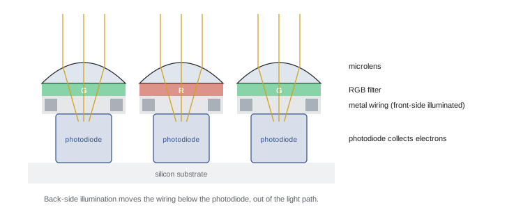
Two quantities describe how efficiently a photosite converts light. Quantum efficiency (QE) is the fraction of incoming photons that produce collected electrons; modern sensors reach 50 to 80 % or more at their peak wavelengths. Fill factor is the fraction of the photosite's area that is actually light-sensitive, since part of each photosite is occupied by transistors and wiring. Microlenses, tiny lenses formed above each photosite, focus light that would fall on non-sensitive areas into the photodiode, effectively raising the fill factor close to 100 %.
Full-well capacity and saturation
A photodiode can hold only a limited number of electrons, its full-well capacity, typically tens of thousands of electrons for cinema camera photosites, and more for larger photosites. When the well fills, further light produces no further signal: the photosite saturates, and that part of the image clips to pure white with no detail. Full-well capacity therefore sets the upper limit of the sensor's dynamic range. Larger photosites generally have larger full-well capacities, which is one reason large photosites are associated with better highlight handling and dynamic range.
Noise
Every measurement contains noise, random variation that obscures the signal. Sensor noise comes from several sources:
- Photon shot noise: light itself arrives randomly, so a photosite receiving an average of \(N\) photons will actually collect a number that varies by about \(\sqrt{N}\) from frame to frame. Shot noise is a property of light, not of the sensor, and dominates in bright areas.
- Read noise: random variation added by the readout circuits and ADC each time a photosite is measured, typically a few electrons in modern sensors. It dominates in the darkest areas.
- Dark current: electrons generated by heat rather than light, which increase with temperature and exposure time.
- Fixed pattern noise: small, consistent differences between photosites or columns, which appear as patterns and are corrected by calibration (black shading).
The signal-to-noise ratio (SNR) describes image quality at a given brightness. Because shot noise grows as the square root of the signal, SNR in bright areas also grows as the square root of the signal: collecting four times as much light doubles the SNR. This is the fundamental reason why more light, whether from larger photosites, larger sensors, wider apertures or brighter scenes, produces cleaner images.
Here \(S\) is the signal in electrons, \(\sigma_{\text{read}}\) the read noise and \(D\) the dark current contribution. When \(S\) is large, \(\text{SNR} \approx \sqrt{S}\); when \(S\) is small, read noise dominates.
Engineering dynamic range
A sensor's engineering dynamic range is the ratio between the largest signal it can record, the full-well capacity, and the smallest distinguishable signal, usually taken as the read noise. Expressed in photographic stops, each a doubling of light:
Worked problem
Calculating engineering dynamic range
A sensor has a full-well capacity of 40,000 electrons and a read noise of 3 electrons. What is its engineering dynamic range in stops? How much would it improve if a dual-gain readout reduced effective read noise to 1.5 electrons while keeping the full well?
Show solution
- Ratio: 40,000 / 3 = 13,333.
- Stops: \(\log_2 13{,}333 \approx 13.7\).
- With 1.5 electrons: 40,000 / 1.5 = 26,667, and \(\log_2 26{,}667 \approx 14.7\).
- Halving the read noise adds one stop.
Answer: About 13.7 stops, rising to about 14.7 stops with the lower read noise.
Engineering dynamic range is an upper bound. In practice, the darkest stops are too noisy to be useful, so the usable dynamic range, which depends on an acceptable SNR threshold, is lower. Manufacturers' claims often use different thresholds, which is why claimed figures vary so widely. Lesson 9 and CINE-202 return to dynamic range in practice.
Readout and analogue-to-digital conversion
At the end of each exposure, the charge in each photosite must be measured. In a CMOS sensor, each photosite contains its own amplifier transistor that converts charge into a voltage. Rows of photosites are selected in turn and their voltages passed down column lines to amplifiers and ADCs at the edge of the sensor, often one ADC per column, which convert them into digital values. The analogue gain applied before conversion, which sets how many electrons correspond to each digital step, is one of the factors behind ISO settings (Lesson 8).
The ADC's bit depth determines how many distinct levels it can produce: 12 bits give 4,096 levels, 14 bits 16,384 and 16 bits 65,536. The bit depth must be high enough to represent the sensor's full range finely without introducing visible steps, but extra bits beyond the noise level add data without adding information. Many cinema sensors digitize at 12 to 16 bits and then encode the result in a smaller number of bits using a logarithmic curve (Lesson 9).
Readout speed matters for several reasons. A sensor that reads out quickly reduces rolling shutter distortion (Lesson 7), allows higher frame rates, and consumes more power and produces more heat. The total data rate leaving a sensor is enormous: a 4.6K sensor with 12 million photosites read at 12 bits and 120 frames per second produces about 17 gigabits per second, which must be processed in real time.
CMOS and CCD sensors
Two sensor technologies dominated digital imaging. Charge-coupled devices (CCDs) shift the charge from each photosite across the chip, bucket-brigade fashion, to a small number of output amplifiers. CCDs offered low noise and uniformity and were used in early digital cinema and broadcast cameras, often in three-chip designs with a prism splitting light into red, green and blue. Complementary metal-oxide-semiconductor (CMOS) sensors place amplifiers in every photosite and integrate readout circuitry, ADCs and even processing on the chip. They are faster, consume less power and are cheaper to manufacture in the same processes used for other chips. CMOS sensors improved rapidly from the mid-2000s and now dominate almost all cameras, from smartphones to the largest cinema cameras.
Modern sensor design features
Several developments have pushed CMOS sensor performance forward:
- Back-side illumination (BSI): the wafer is flipped and thinned so that light enters from the back, with the wiring layers below the photodiodes rather than above them, increasing the light collected, especially for small photosites.
- Stacked sensors: the photodiode layer is bonded to a separate logic layer containing readout circuitry and memory, allowing much faster readout and more processing on the sensor.
- Dual-gain and dual conversion gain readout: each photosite can be read with two different gains, either switched between modes (dual native ISO) or read simultaneously and combined, extending dynamic range (Lesson 8).
- Improved microlenses and colour filters that reduce crosstalk between neighbouring photosites.
- Global shutter designs that store each photosite's charge in an in-pixel memory so that all photosites expose at the same instant (Lesson 7).
| Feature | What it improves | Trade-off |
|---|---|---|
| Microlenses | Effective fill factor, sensitivity | Can cause angle-dependent colour shifts with some lenses |
| Back-side illumination | Light collection, especially small pixels | More complex manufacturing |
| Stacked construction | Readout speed, frame rates, rolling shutter | Cost, heat |
| Dual-gain readout | Dynamic range, low-light performance | Processing complexity |
| Global shutter | Eliminates rolling shutter artefacts | Historically more noise and less dynamic range |
Photosite size and its consequences
Photosite size, also called pixel pitch, is the distance between neighbouring photosites, typically between about 3 and 9 micrometres in cinema cameras. For a given sensor size, more photosites means smaller photosites. Smaller photosites hold fewer electrons and collect less light each, but there are more of them, and when the image is viewed at the same final size, the total light collected by the sensor is what matters most for noise. Modern sensors show that high resolution and good noise performance can coexist, especially when oversampled images are scaled down. Larger photosites still tend to offer higher full-well capacity and dynamic range per photosite, and in some designs better highlight handling.
Spectral response
A photosite's quantum efficiency varies with wavelength. Silicon responds from the ultraviolet through the visible spectrum and well into the near infrared, up to about 1,100 nanometres, far beyond what the eye can see. This is why cameras need infrared-cut filters: without them, infrared light from tungsten lamps, sunlight and some fabrics would be recorded as visible colour, making black fabrics look brown or magenta and foliage look unnatural. Strong ND filters that cut visible light but pass infrared can cause the same problem, which is why cinema-grade ND filters include infrared control. Some cameras are deliberately converted for infrared photography by removing the infrared-cut filter.
Linearity and the response curve
Within its working range, a sensor's response is very linear: twice the light gives twice the signal. Near saturation, the response may bend slightly before clipping, and at the very bottom, the signal is buried in noise. This linearity is what makes raw sensor data so useful for visual effects, where light must be added and combined accurately. It also means that all the "character" of a camera's tonal response, its contrast curve and highlight roll-off, comes from processing rather than from the sensor itself, unlike film, whose chemistry gave it a characteristic S-shaped curve.
Blooming and smear
When a photosite overflows, excess charge can spill into neighbouring photosites, producing blooming around very bright sources. Older CCD sensors were also prone to vertical smear, bright streaks above and below highlights caused by charge passing through the readout registers during light exposure. Modern CMOS sensors include anti-blooming structures that drain excess charge, and smear is rare, but extreme highlights such as the sun in frame can still produce artefacts such as dark centres or coloured fringes, worth testing with any new camera.
Hot pixels and defect correction
Among millions of photosites, some are defective: stuck at high values (hot pixels), at zero (dead pixels) or unusually sensitive. Manufacturers map defective photosites at the factory and the camera replaces their values with interpolated ones. New hot pixels can appear over time, particularly after exposure to cosmic radiation during air travel. Many cameras include a pixel remapping routine that the camera team can run, and checking for hot pixels with the lens capped at the start of a production is good practice.
Why sensor knowledge matters on set
Knowing how sensors work turns abstract specifications into practical decisions: giving the sensor enough light to keep shot noise low, keeping the camera cool on long takes, recalibrating after temperature changes, and protecting highlights from clipping because saturated photosites contain no recoverable detail.
Common mistakes
MistakeAttributing all noise to the sensor.
InsteadPhoton shot noise comes from light itself; more light means less noise.
MistakeTreating engineering dynamic range as usable range.
InsteadUsable range is lower, depending on acceptable noise.
MistakeAssuming more bits always means more information.
InsteadBits beyond the noise level add data, not detail.
MistakeAssuming high resolution always means more noise.
InsteadCompare noise at the same viewing size.
MistakeIgnoring sensor temperature.
InsteadKeep sensors cool and calibrated to reduce dark current and patterns.
Summary and key terms
- Photosites convert photons to electrons by the photoelectric effect.
- Quantum efficiency and fill factor describe conversion efficiency; microlenses help.
- Full-well capacity sets the saturation point and upper dynamic range limit.
- Noise sources include shot noise, read noise, dark current and fixed pattern noise.
- Engineering dynamic range is log₂(full well / read noise).
- CMOS sensors with column ADCs dominate modern cameras.
- BSI, stacking, dual gain and global shutter advance sensor performance.
- Photodiode
- Silicon structure collecting freed electrons.
- Quantum efficiency
- Fraction of photons producing electrons.
- Fill factor
- Light-sensitive fraction of a photosite.
- Microlens
- Tiny lens focusing light into a photosite.
- Full-well capacity
- Maximum electrons a photosite holds.
- Shot noise
- Random variation in photon arrival.
- Read noise
- Noise added during readout.
- Dark current
- Heat-generated electrons.
- CMOS
- Sensor type with per-photosite amplifiers.
- Back-side illumination
- Light entering from the wafer's back side.
Practice problems
Work each problem on paper first, then reveal the answer to check.
What converts light to charge in a photosite?
Show answer
The photoelectric effect in the photodiode.
What does quantum efficiency measure?
Show answer
The fraction of photons that produce collected electrons.
What happens when a photosite reaches full well?
Show answer
It saturates and clips to white.
Shot noise for an average of 10,000 photons?
Show answer
About 100 (√10,000).
SNR change when light increases fourfold (shot-noise limited)?
Show answer
It doubles.
Engineering DR for 60,000 e⁻ full well and 2 e⁻ read noise?
Show answer
log₂ 30,000 ≈ 14.9 stops.
Levels in a 14-bit ADC?
Show answer
16,384.
Why did CMOS replace CCD?
Show answer
Faster readout, lower power, integrated circuitry, lower cost.
What does a stacked sensor add?
Show answer
A separate logic layer for fast readout and processing.
What does black shading correct?
Show answer
Fixed pattern noise and black level variation.
Lesson quiz · 5 questions
Score 60% or more to complete this lesson.
Create a free account to save your progress, take quizzes and earn a certificate.