
ELE-499 · Lesson 5 of 12 · 21 min
Power electronics design
The laboratory demonstrator is the part of Concept B that the team chose to build: a bidirectional DC-DC converter that moves power between a battery and a 400 V DC bus. In the full common-bus design it would connect the battery cabinet to an 800 V bus at 100 kW. For the demonstrator Aisha scaled it to 6 kW, a 204.8 V nominal lithium iron phosphate laboratory battery and a 400 V bus, a size that could be built on a bench, tested safely with the university's equipment and still exercise every real design problem. This lesson follows her design from topology to heat sink, drawing on the methods of ELE-470.
Converter requirements
Aisha began with a derived requirement sheet. The converter shall transfer up to 6 kW in either direction between a battery of 160 V to 233 V and a bus regulated at 400 V; shall achieve at least 97.5 % efficiency from 30 % to 100 % of rated power (requirement R5); shall keep inductor current ripple below 40 % of the phase current; shall limit battery current to 32 A; shall pre-charge the bus capacitors before closing its contactor; shall shut down safely on overcurrent, overvoltage, overtemperature or loss of control; and shall be controllable over a serial link from the site energy controller. Each line traces to a top-level requirement or to safe operation.
Choosing the topology
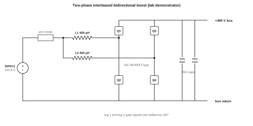
Because the bus voltage is always higher than the battery voltage, a non-isolated boost converter run in both directions is the natural choice. In boost mode, power flows from the battery to the bus; in buck mode, with the other switch active, power flows from the bus to the battery. Replacing the boost diode with a second transistor makes the converter synchronous and bidirectional, and lowers conduction loss.
Aisha considered three alternatives. An isolated dual active bridge would provide galvanic isolation and handle a wider voltage ratio, but it doubles the number of switches and adds a transformer, too much for one term. A single-phase boost would need one large inductor carrying the whole 30 A with high ripple current in the capacitors. A two-phase interleaved boost splits the current between two smaller inductors switched 180° apart, so that their ripple currents partly cancel at the capacitors and the effective ripple frequency doubles. She chose two-phase interleaving, which also lets each phase use smaller, cheaper magnetics and spreads the heat.
Semiconductors
At 400 V and 50 kHz, the choice is between silicon IGBTs, silicon superjunction MOSFETs and silicon carbide (SiC) MOSFETs. IGBTs are robust and cheap but their switching losses climb steeply above about 20 kHz, and they have a fixed on-state voltage that wastes power at light load. Silicon MOSFETs switch fast, but their body diodes recover slowly, which causes large losses in a synchronous half-bridge where each body diode conducts during the dead time. SiC MOSFETs combine fast switching with a body diode that has very little reverse-recovery charge, which is why they have become standard in electric vehicle and storage converters. Aisha chose 650 V SiC MOSFETs, which give about 250 V of margin over the bus to allow for switching overshoot.
A rating of 650 V for a 400 V bus may seem generous. It is not. When a transistor turns off quickly, the stray inductance of the loop formed by the switches and the bus capacitors produces a voltage spike, and the drain-source voltage can overshoot the bus by 50 to 100 V. Designers commonly keep the bus at no more than about two-thirds of the device rating, both for spikes and because cosmic-ray-induced failures in power devices rise with applied voltage.
Duty cycle, ripple and the inductor
In continuous conduction, an ideal boost converter's duty cycle is D = 1 − Vbattery / Vbus, so at the nominal 204.8 V and 400 V the duty cycle is about 0.49. Each phase carries half of the 29 A battery current at full power, 14.6 A. The inductor ripple current is Δi = Vbattery · D / (L · fsw). Aisha's first estimate used 220 µH per phase, which gave about 9 A of ripple, 62 % of the phase current, far above her 40 % target. Increasing the inductance to 400 µH brought the ripple down to about 5 A, 34 %.
Worked problem
Inductance for a ripple target
A boost phase runs from 204.8 V at D = 0.488 and 50 kHz. What inductance gives 5.0 A peak-to-peak ripple?
Show solution
- \[L = \dfrac{V_{batt}\,D}{\Delta i\, f_{sw}}\]
- \[L = \dfrac{204.8 \times 0.488}{5.0 \times 50\,000} \approx 400\ \mu\text{H}\]
Answer: About 400 µH per phase.
The inductors were custom wound on powdered-iron alloy toroids. Powdered cores have a distributed air gap, so they store energy without a discrete gap and saturate softly, which suits a converter that might see current transients. Aisha checked three things: that the peak flux density at the 32 A current limit stayed well below saturation, allowing for the fact that powdered cores lose permeability as current rises; that winding resistance at full current gave acceptable copper loss; and that core loss at 50 kHz and the operating ripple stayed within a few watts per inductor. She used the core manufacturer's published loss curves, and recorded every assumption in her logbook.
Capacitors and the bus
The bus capacitors absorb the pulsed current from the switching legs and hold the bus steady during load steps. Film capacitors are preferred over electrolytics at this voltage and frequency because they handle high ripple current, have low equivalent series resistance and age slowly. Interleaving halves the effective ripple current the capacitors must carry, compared with a single phase. Aisha sized the bank for its ripple current rating rather than its capacitance, which is common in fast-switching converters: six 20 µF film capacitors gave enough ripple-current capacity with margin, and their total capacitance kept bus ripple below 1 %.
Losses and efficiency
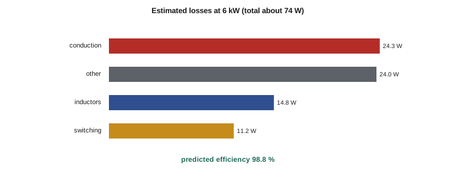
Efficiency is the converter's headline requirement, and it is decided by losses in four places: conduction loss in the transistors, switching loss each time a transistor turns on or off, copper and core loss in the inductors, and everything else, which includes gate drive, sensing, capacitor ESR and control power. The program estimates each at full power from datasheet values, using the hot on-resistance of the MOSFETs, since resistance rises with temperature, and scaling the datasheet's switching energy to the operating voltage and current.
# Two-phase interleaved bidirectional boost for the lab demonstrator: losses, efficiency and heat sink
import math
P, VB, VBUS, FSW, N = 6000.0, 204.8, 400.0, 50e3, 2       # W, battery V, bus V, switching Hz, phases
RDS, ESW_REF, VREF, IREF = 0.040 * 1.4, 115e-6, 400.0, 15.0 # hot on-resistance; switching energy per cycle at ref point
L_UH, RL, CORE_W = 400e-6, 0.018, 3.5                     # inductance per phase, winding ohms, core loss per inductor
D = 1 - VB / VBUS
I_ph = P / VB / N
ripple = VB * D / (L_UH * FSW)                            # peak-to-peak inductor ripple, A
i_rms_l = math.sqrt(I_ph ** 2 + ripple ** 2 / 12)
p_cond = N * (RDS * i_rms_l ** 2)                          # one switch conducts at a time per phase (synchronous)
p_sw = N * ESW_REF * (VBUS / VREF) * (I_ph / IREF) * FSW
p_ind = N * (RL * i_rms_l ** 2 + CORE_W)
p_misc = 0.004 * P                                         # gate drive, sensing, capacitor ESR, control
loss = p_cond + p_sw + p_ind + p_misc
print(f"duty {D:.3f}, phase current {I_ph:.1f} A, ripple {ripple:.1f} A pp ({ripple / I_ph * 100:.0f} %)")
print(f"conduction {p_cond:.1f} W, switching {p_sw:.1f} W, inductors {p_ind:.1f} W, other {p_misc:.1f} W")
print(f"total loss {loss:.1f} W -> efficiency {P / (P + loss) * 100:.2f} % at 6 kW")
# heat sink: all four MOSFETs on one sink, keep the junction at or below 125 C in 40 C air
TA, TJ_MAX, RJC, RCS = 40.0, 125.0, 0.65, 0.30
p_dev = (p_cond + p_sw) / (2 * N)                          # per device, two devices per phase
t_case_allowed = TJ_MAX - p_dev * (RJC + RCS)
r_sa = (t_case_allowed - TA) / (p_cond + p_sw)
print(f"per-device loss {p_dev:.1f} W; sink must stay below {t_case_allowed:.0f} C -> sink-to-air <= {r_sa:.2f} K/W")duty 0.488, phase current 14.6 A, ripple 5.0 A pp (34 %) conduction 24.3 W, switching 11.2 W, inductors 14.8 W, other 24.0 W total loss 74.3 W -> efficiency 98.78 % at 6 kW per-device loss 8.9 W; sink must stay below 117 C -> sink-to-air <= 2.16 K/W
The estimate gave about 74 W of loss at 6 kW, an efficiency of about 98.8 %. Conduction loss is the largest single item at about 24 W, followed by the \"other\" allowance of 24 W, inductor loss of about 15 W and switching loss of about 11 W. Two lessons follow. First, SiC has made switching loss a minor term at this frequency, so a higher switching frequency, with smaller inductors, would be possible. Second, the \"other\" allowance, 0.4 % of rated power, is a guess, and at light load it dominates. Lesson 10 shows what the measurements said, and why Aisha's estimate turned out optimistic by about half a percentage point.
Thermal design
Loss becomes heat, and heat sets the size of the heat sink. The program places all four MOSFETs on one sink and works backwards from a junction limit of 125 °C, chosen below the device's 175 °C rating for reliability, at 40 °C ambient. With about 9 W per device, a junction-to-case thermal resistance of 0.65 K/W and 0.30 K/W across the thermal interface, the sink itself must stay below about 117 °C, which requires a sink-to-air thermal resistance of no more than about 2.2 K/W for the 36 W the four devices dissipate. A modest extruded sink with a small fan meets that easily. Aisha nonetheless chose a sink with about twice the needed performance, because thermal resistance figures in catalogs assume ideal airflow and mounting, and because a cooler junction lengthens device life.
The inductors are cooled separately, by convection and the same fan, and their temperature rise was estimated from their surface area and loss. Lesson 10 checks all of these estimates in a heat run.
Gate drive, protection and sequencing
Each MOSFET is driven by an isolated gate driver, because the high-side switch's source moves between 0 and 400 V every cycle, and because isolation keeps power-stage noise out of the control circuits. SiC MOSFETs need higher gate voltages than silicon, typically about +18 V to turn on and a few volts negative to hold them off against noise. A dead time of about 100 ns between the two switches in each leg prevents shoot-through, a short circuit across the bus. The driver has desaturation detection, which senses an abnormally high drain voltage during conduction and turns the device off within microseconds of a short circuit.
The protection hierarchy has three layers. The gate drivers' desaturation detection handles short circuits in microseconds. A hardware comparator on each current-sense signal trips the drivers if phase current exceeds the limit, independently of the microcontroller. And the firmware handles slower faults, such as overtemperature, battery out of range or loss of communication, by ramping power down in an orderly way. The bus capacitors are pre-charged through a resistor before the main contactor closes, to avoid a large inrush current that would weld the contactor or stress the battery. A bleed resistor discharges the bus to a safe voltage within a minute of shutdown, so that nobody opens the enclosure onto charged capacitors.
Bidirectional operation and control
In boost mode the converter regulates bus voltage while drawing current from the battery; in buck mode it charges the battery with a current set by the site energy controller, within limits set by the battery management system. Each phase has its own inner current loop, so that the two phases share current equally despite small differences in inductance; an outer loop sets the total. The control design is the subject of lesson 7.
Common mistakes
MistakeChoosing a device voltage rating just above the bus voltage.
InsteadAllow for switching overshoot; keep the bus at about two-thirds of the rating or less.
MistakeSizing film capacitors by capacitance alone.
InsteadCheck ripple-current rating; it usually decides the bank.
MistakeUsing the room-temperature on-resistance in loss estimates.
InsteadOn-resistance rises with temperature; use the hot value.
MistakeTrusting firmware alone for overcurrent protection.
InsteadAdd hardware comparators and gate-driver desaturation detection that act without the microcontroller.
Summary and key terms
- A bidirectional synchronous boost moves power between a battery and a higher-voltage bus.
- Interleaving two phases reduces capacitor ripple current and spreads losses.
- SiC MOSFETs suit 400 V converters at tens of kilohertz because of low switching and recovery losses.
- Inductance is chosen from the ripple target: L = V·D/(Δi·f).
- Efficiency is decided by conduction, switching, magnetic and miscellaneous losses.
- The heat sink is sized backwards from a junction limit, with margin for real airflow.
- Protection has hardware and firmware layers, plus pre-charge and bus discharge.
- Interleaving
- Operating parallel converter phases with shifted switching times so their ripple currents partly cancel.
- Synchronous rectification
- Replacing a diode with a controlled transistor to reduce conduction loss.
- Dead time
- A short interval when both switches in a leg are off, to prevent shoot-through.
- Desaturation detection
- Gate-driver protection that turns a transistor off if its voltage rises abnormally while conducting.
- Pre-charge
- Charging capacitors through a resistor before closing a main contactor.
- Thermal resistance
- Temperature rise per watt of heat flow through a path, in K/W.
- Ripple current
- The alternating component of current in an inductor or capacitor.
Practice problems
Work each problem on paper first, then reveal the answer to check.
What is the duty cycle of an ideal boost from 204.8 V to 400 V?
Show answer
D = 1 − 204.8/400 ≈ 0.49.
Why does interleaving help the capacitors?
Show answer
The phases' ripple currents partly cancel and the ripple frequency doubles.
Why not use silicon MOSFETs in the synchronous half-bridge?
Show answer
Their body diodes have large reverse recovery, causing high losses.
A device dissipates 9 W with 0.95 K/W from junction to sink. If the junction must stay at 125 °C, what is the maximum sink temperature?
Show answer
About 116 °C.
Name the three protection layers in the converter.
Show answer
Gate-driver desaturation, hardware overcurrent comparators, firmware protection.
Why is the bus pre-charged before the contactor closes?
Show answer
To limit inrush current that could weld the contactor or stress the battery.
Lesson quiz · 5 questions
Score 60% or more to complete this lesson.
Create a free account to save your progress, take quizzes and earn a certificate.