
ELE-499 · Lesson 9 of 12 · 22 min
Prototyping, printed circuit boards and the build
Week sixteen was the turning point of the year. The design was approved, and the team had nine weeks to turn files into working hardware, test it and report. Building is where capstone schedules usually break, because it depends on suppliers, fabricators and lab time that the team does not control, and because the first board almost never works the first time. This lesson covers how Aisha and Mateo laid out the converter's printed circuit board, the design rules that kept it safe and buildable, the budget and ordering, assembly, and the step-by-step bring-up that turned a bare board into a working converter.
Ordering before the design is finished
The team had learned the most important build lesson early, from Professor Gagnon's warning at the PDR: some parts take longer to arrive than the build phase lasts. In week ten, before the CDR, Aisha checked the lead time of every component that was not a common stock item. The SiC MOSFETs and isolated gate drivers were in stock at distributors. The custom inductors, wound by a small local magnetics shop, quoted six weeks. The film capacitors had a four-week lead time. The laboratory battery and its management system had been borrowed from the department's energy lab, and the 400 V supply and electronic load from Cedarline's test bay. She ordered the inductors and capacitors at risk, before the CDR approved the design, because their specifications were settled and waiting would have used up the build phase. The risk register recorded this decision and its cost if the design changed.
Board stack-up and the power loop
The converter board is a four-layer board with 2 oz copper on every layer. The outer layers carry the power traces and components; one inner layer is a solid ground plane for the control circuits, and the other carries the bus return and wide power connections. Thick copper keeps the power traces' resistance and temperature rise low without making them impractically wide.
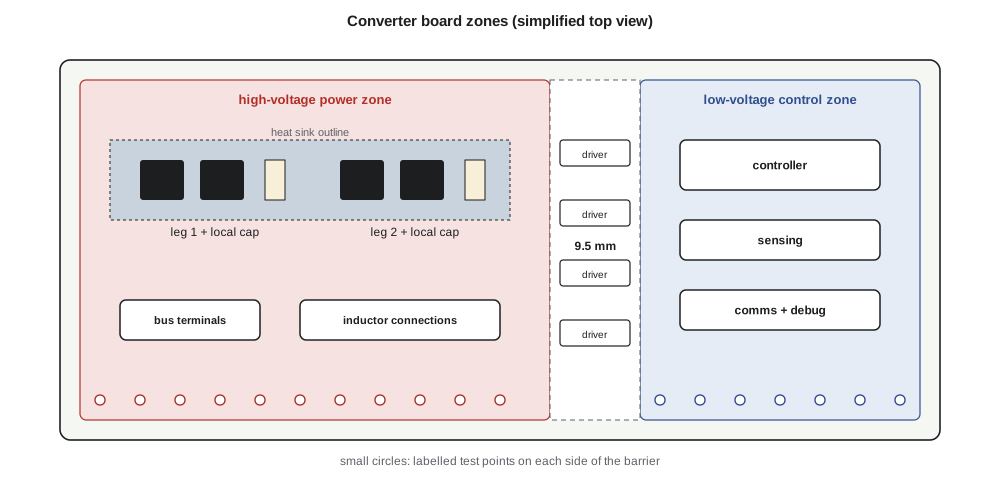
The most important layout decision in any fast-switching converter is the power commutation loop: the path from the bus capacitor, through the high-side and low-side transistors of a leg, and back to the capacitor. Every nanohenry of inductance in that loop adds voltage overshoot at turn-off, as the simulation in lesson 8 showed. Aisha placed a small, low-inductance film capacitor directly across each leg, right beside the two MOSFETs, and routed the bus positive and return on adjacent layers directly above one another, so that their magnetic fields cancel. Her estimate of the loop inductance fell from about 25 nH in her first placement to under 10 nH.
Gate drive layout matters almost as much. Each MOSFET has a separate Kelvin source pin, which returns the gate current through its own path rather than through the power source connection, so that the large switching current does not induce a voltage that fights the gate drive. Each gate driver sits as close to its MOSFET as possible, with its isolated supply and decoupling capacitors next to it, and the gate loop is kept small.
Trace widths and spacing
A trace's width must carry its current without excessive temperature rise. The traditional sizing method comes from charts in IPC-2221, the generic printed board design standard, which relate current, temperature rise and copper cross-section; the program below uses a widely quoted curve fit to those charts. Inner layers need wider traces than outer layers for the same current, because they cannot shed heat to the air. Modern guidance, in IPC-2152, gives more accurate and usually less conservative values, so Aisha treated the older fit as a quick upper bound and confirmed the critical traces with the fabricator's calculator.
# PCB design checks for the converter board: trace width (IPC-2221 curve fit), spacing table and a bill of materials
import math
def width_mm(i, rise_c, oz, external=True):
    k = 0.048 if external else 0.024
    area_mil2 = (i / (k * rise_c ** 0.44)) ** (1 / 0.725)
    thick_mil = 1.378 * oz
    return area_mil2 / thick_mil * 0.0254
for net, amps in (('phase inductor', 17.5), ('battery input', 32.0), ('DC bus', 16.0), ('gate drive', 1.0)):
    print(f"{net:15s} {amps:5.1f} A: outer layer {width_mm(amps, 20, 2):5.1f} mm, inner layer {width_mm(amps, 20, 2, False):5.1f} mm (2 oz, 20 C rise)")
# team design-rule spacings (taken from the safety standard and the fabricator's capability; see the lesson)
rules = [('400 V bus to low-voltage control (reinforced)', 8.0, 9.5), ('400 V bus to chassis (basic)', 4.0, 5.0),
         ('battery + to battery -', 2.5, 3.2), ('control nets', 0.15, 0.20)]
for name, need, laid in rules:
    print(f"{name:46s} required {need:4.2f} mm, layout {laid:4.2f} mm  {'ok' if laid >= need else 'FAIL'}")
bom = [('SiC MOSFETs', 4, 18.40), ('gate drivers, isolated', 4, 6.90), ('inductors, custom', 2, 64.00),
       ('film capacitors, bus', 6, 11.20), ('controller board', 1, 85.00), ('heat sink and fan', 1, 72.00),
       ('PCB, 4 layer 2 oz', 1, 96.00), ('current shunt and amplifier', 2, 9.50), ('connectors and hardware', 1, 58.00)]
total = sum(q * c for _, q, c in bom)
for n, q, c in bom: print(f"  {n:28s} {q:2d} x {c:6.2f} = {q * c:7.2f}")
print(f"prototype parts per board: {total:.2f} dollars; two boards plus 15 % spares and shipping: {2 * total * 1.15:.0f} dollars")phase inductor 17.5 A: outer layer 5.1 mm, inner layer 13.3 mm (2 oz, 20 C rise) battery input 32.0 A: outer layer 11.7 mm, inner layer 30.6 mm (2 oz, 20 C rise) DC bus 16.0 A: outer layer 4.5 mm, inner layer 11.7 mm (2 oz, 20 C rise) gate drive 1.0 A: outer layer 0.1 mm, inner layer 0.3 mm (2 oz, 20 C rise) 400 V bus to low-voltage control (reinforced) required 8.00 mm, layout 9.50 mm ok 400 V bus to chassis (basic) required 4.00 mm, layout 5.00 mm ok battery + to battery - required 2.50 mm, layout 3.20 mm ok control nets required 0.15 mm, layout 0.20 mm ok SiC MOSFETs 4 x 18.40 = 73.60 gate drivers, isolated 4 x 6.90 = 27.60 inductors, custom 2 x 64.00 = 128.00 film capacitors, bus 6 x 11.20 = 67.20 controller board 1 x 85.00 = 85.00 heat sink and fan 1 x 72.00 = 72.00 PCB, 4 layer 2 oz 1 x 96.00 = 96.00 current shunt and amplifier 2 x 9.50 = 19.00 connectors and hardware 1 x 58.00 = 58.00 prototype parts per board: 626.40 dollars; two boards plus 15 % spares and shipping: 1441 dollars
The phase inductor traces need about 5 mm on an outer layer for 17.5 A, including ripple, at a 20 °C rise, and the battery input about 12 mm for 32 A. Rather than use such wide outer traces, Aisha used copper pours on both outer layers in parallel, stitched with many vias, and brought the battery current onto the board through screw terminals placed close to the inductors so that the high-current path is short.
Spacing is a safety matter. Two distances matter between conductors at different voltages: clearance, the shortest path through air, which protects against flashover; and creepage, the shortest path along the board surface, which protects against tracking across contamination and moisture. Safety standards set minimum values depending on the working voltage, the pollution degree of the environment, the board material and whether the insulation is basic, protecting against a single fault, or reinforced, providing the protection of two independent layers. The control circuits and communication ports, which connect to the site controller and could be touched during testing, must be separated from the 400 V bus by reinforced insulation. Hannah derived the team's spacing rules from the tables of the relevant equipment safety standard for the working voltage and pollution degree, and Aisha laid out the board with margin above each. The isolation barrier between the power and control zones is 9.5 mm wide against an 8 mm requirement, and the gate drivers and current-sense amplifiers that cross it are isolated components rated for reinforced insulation.
Worked problem
Inner versus outer
Using the curve fit I = k·ΔT^0.44·A^0.725, with k = 0.048 for outer and 0.024 for inner layers, how much more copper cross-section does an inner trace need than an outer one for the same current and temperature rise?
Show solution
- For equal I and ΔT, A^0.725 must double when k halves.
- \[A_{inner}/A_{outer} = 2^{1/0.725} \approx 2.6\]
Answer: About 2.6 times the cross-section, so about 2.6 times the width at the same copper thickness.
Designing for test and assembly
Mateo insisted on test points before layout was released. Every power rail, every gate signal, both current-sense outputs, the bus voltage sense and the main control signals have a labelled test point, and the low-voltage test points are on the control side of the barrier so that they can be probed safely. The board has a header for the controller's debugger, a set of status LEDs, and a jumper that disables the gate drivers so that the control circuits can be tested without the power stage. These cost a few square centimetres of board and saved days during bring-up.
Design for manufacture and assembly means checking that the fabricator can make the board and the assembler can build it. The team's fabricator published minimum trace widths and spacings, via sizes and copper weights; the design rules in the layout tool were set to those values, and a design rule check ran clean before release. Components were chosen in packages the university's assembly lab could place and reflow, and polarized parts were marked clearly on the silkscreen. The bill of materials listed manufacturer part numbers, not just values, with an approved alternative for each part that had one.
Budget
The department gave each capstone team a parts budget, and Larchmont contributed an additional sum for the demonstrator. The program's bill of materials totals about 626 dollars per board for the main parts. Aisha ordered parts for two boards plus spares, about 1,440 dollars with shipping, because the first board in any prototype run is likely to be damaged during bring-up. That proved wise: one MOSFET and one gate driver on the first board were lost to a probing mistake described below. Every purchase was logged against the budget, and the earned value report in lesson 12 includes the money as well as the hours.
Assembly and inspection
The boards arrived bare in week nineteen. Aisha and Mateo assembled the control section first, in the university's lab, and inspected it under a microscope before powering anything. Inspection found one problem: the footprint for one of the isolated DC-DC converters that supply the gate drivers had been drawn from a top view of the package when the datasheet showed a bottom view, so its pins were mirrored. Two minutes with a continuity tester confirmed it before power was applied. The fix on the first board was a small adapter; the second board's layout was corrected and the change was recorded as revision B. Footprint errors are one of the most common board problems, and the cure is a second person checking every new footprint against the datasheet drawing before release.
Bring-up in stages
Bring-up followed a written procedure that Hannah reviewed. The principle is to apply power in steps, each with a current-limited supply and a stop condition, so that a fault damages as little as possible. First the control section was powered from a bench supply at its normal low voltage with the current limit set just above its expected draw, and its rails and clocks were checked. Then the controller was programmed and its communications tested. Then the gate drivers were powered and their outputs checked with the power stage unpowered, confirming the correct gate voltages, dead times and the 180° phase shift between legs. Only then was the power stage connected to a low DC voltage, about 30 V, through a current-limited supply with a small resistive load, and operated in open loop at a fixed duty cycle. The voltage was raised in steps to 100 V, 200 V and finally the full 400 V bus, checking waveforms and temperatures at each step, before the closed loops were enabled and the battery was connected.
The probing mistake happened at the 100 V step. Mateo connected a ground-referenced oscilloscope probe's ground lead to the switching node of a leg, contrary to the safety plan. The scope's ground clip shorted the low-side MOSFET through the oscilloscope's earth connection. The current-limited supply and the desaturation protection limited the damage to one MOSFET and one gate driver, and nobody was hurt, but the team stopped work for the day, reported it to the advisor and the lab safety officer, and reviewed the procedure. From then on, every switching-node measurement used a high-voltage differential probe, and the procedure step was rewritten to say so explicitly. Reporting a near miss, rather than quietly replacing the parts, is part of professional practice.
Common mistakes
MistakeOrdering long-lead parts after the design review.
InsteadCheck lead times early and order settled parts at risk, recording the decision.
MistakeLaying out a fast converter without minimizing the commutation loop.
InsteadPlace local capacitors beside the switches and overlap bus traces to cancel inductance.
MistakeSkipping test points to save board area.
InsteadLabelled test points and a gate-disable jumper save days in bring-up.
MistakePowering a new board at full voltage.
InsteadBring up in stages with current-limited supplies and stop conditions.
Summary and key terms
- Check lead times early; order settled long-lead parts at risk.
- Minimize power-loop inductance with local capacitors and overlapping bus layers.
- Use Kelvin source connections and short gate loops.
- Size traces for temperature rise; inner layers need more copper than outer layers.
- Clearance and creepage, basic or reinforced, come from safety standard tables for the working voltage and environment.
- Design for test and assembly: test points, debug access, fabricator rules and checked footprints.
- Bring up in stages with current limits, and report near misses.
- Commutation loop
- The current path through a switching leg and its bus capacitor during a transition.
- Kelvin source
- A separate source connection used only for the gate-drive return.
- Clearance
- The shortest distance through air between conductors.
- Creepage
- The shortest distance along an insulating surface between conductors.
- Reinforced insulation
- Insulation providing protection equivalent to two independent layers.
- Design for manufacture (DFM)
- Designing so that a product can be made reliably with available processes.
- Bring-up
- The staged process of first powering and testing new hardware.
Practice problems
Work each problem on paper first, then reveal the answer to check.
Why place a small film capacitor beside each leg?
Show answer
To keep the commutation loop short and its inductance low.
Why are inner-layer traces wider for the same current?
Show answer
Inner layers cannot shed heat to the air as easily.
What is the difference between clearance and creepage?
Show answer
Clearance is through air; creepage is along the surface.
Why did the team order inductors before the CDR?
Show answer
Their six-week lead time would otherwise have consumed the build phase.
What caught the mirrored footprint?
Show answer
Microscope inspection and a continuity check before power-up.
What changed after the probing incident?
Show answer
Differential probes were required for switching-node measurements and the procedure was rewritten.
Lesson quiz · 5 questions
Score 60% or more to complete this lesson.
Create a free account to save your progress, take quizzes and earn a certificate.