
ELE-340 · Lesson 3 of 12 · 24 min
The differential pair
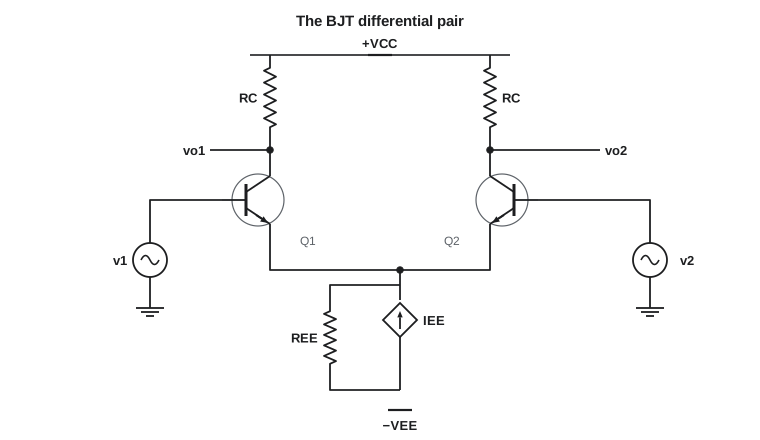
The differential pair is two matched transistors whose emitters, or sources, share a current source. It amplifies the difference between its two input voltages and largely ignores the part they have in common. That one property makes it the input stage of every op amp, comparator and instrumentation amplifier, the heart of balanced line receivers, and the reason a direct-coupled amplifier can be stable against temperature: whatever drifts equally in both transistors cancels. This lesson analyzes the pair for large and small signals, defines common-mode rejection, shows what limits it, and connects the pair to a current-mirror load to make the first stage of an op amp.
For the APS-2, the pair has a practical job. The remote microphone signal comes down a 15 m two-conductor shielded cable that runs beside the street-lighting conductors inside the pole. Leo measures the cable on the bench with a mock-up of the pole wiring: the microphone's own signal appears as a difference of up to 10 mV peak between the two conductors, while 60 Hz hum appears on both conductors together at about 0.5 V peak relative to the station's ground. A single-ended amplifier would amplify the hum fifty times more than the voice-band noise it is supposed to measure. A differential input can reject it.
Differential and common-mode signals
Any two input voltages v_1 and v_2 can be written as a difference and an average. The differential-mode input v_id = v_1 − v_2 is the wanted signal; the common-mode input v_icm = (v_1 + v_2)/2 is what both inputs share, such as hum induced equally in two conductors, ground voltage differences between two pieces of equipment, or the DC bias level. An amplifier's response to each is described by a differential gain A_d and a common-mode gain A_cm, and its quality by the common-mode rejection ratio:
Large-signal behaviour
Because the tail source fixes the sum of the two emitter currents, the pair can only steer current from one side to the other. With the exponential BJT law, the ratio of the two collector currents is e^(v_id/V_T), and the currents are
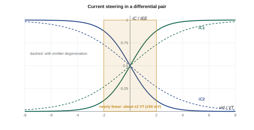
Two facts follow. The pair is linear only for |v_id| below about 2V_T, roughly ±50 mV at room temperature; beyond about ±4V_T, ±100 mV, practically all the current flows on one side, and the pair acts as a current switch. That switching behaviour is useful in comparators and in the class-D modulator of lesson 11. For linear amplification of larger signals, a resistor R_E in each emitter widens the linear range to roughly ±I_EE R_E, at the cost of gain, exactly as degeneration did in a single stage. A MOSFET pair steers current the same way but follows the square law; its linear range is about ±V_ov and full switching occurs at |v_id| = √2 V_ov, so a MOSFET pair biased at a few hundred millivolts of overdrive handles larger signals than an undegenerated BJT pair.
Small-signal differential gain
For small v_id, the emitter node stays still: as one emitter current rises, the other falls by the same amount, so the tail sees no change and acts as a virtual ground for differential signals. Each half of the pair is then a common-emitter stage driven by ±v_id/2. With g_m = (I_EE/2)/V_T for each transistor,
Taking the output between the two collectors gives the full gain g_m R_C; taking it from one collector to ground gives half. The differential input resistance is 2r_π, or 2(β + 1)(r_e + R_E) with degeneration. The half-circuit idea, analyzing one transistor with the tail grounded for differential signals, is the main tool for every symmetrical circuit in this course.
Common-mode gain and CMRR
For a common-mode input, both emitters move together, and the tail current changes by v_icm/R_EE, where R_EE is the output resistance of the tail source. Each side carries half of that change. The common-mode half-circuit is therefore a CE stage with an emitter resistance of 2R_EE, and
A large tail resistance is the key. A resistor tail cannot be very large without dropping too much DC voltage, but a current-mirror tail can have an output resistance of megohms. With a perfectly matched pair and the output taken differentially, the common-mode signals at the two collectors are identical and cancel completely; real CMRR is then limited by mismatch. If the collector resistors differ by a fraction ε, a common-mode input produces a differential output of about ε R_C v_icm/(2R_EE), and the differential CMRR becomes about 2g_m R_EE/ε, very high at DC. At higher frequencies the capacitance across the tail source lowers its impedance, so CMRR falls with frequency, typically 20 dB per decade above a few kilohertz in general-purpose op amps.
Worked problem
Hum rejection with a resistor tail and a current-source tail
A pair runs at I_EE = 1 mA (g_m = 19.3 mS per transistor) with R_C = 10 kΩ and a single-ended output. Compare a 100 kΩ resistor tail with a current-source tail of 2 MΩ output resistance. The inputs carry a 10 mV differential signal and 0.5 V of common-mode hum.
Show solution
- \[A_{d,\text{single}} = \frac{0.0193 \times 10\,000}{2} \approx 96.7\]
- Resistor tail:
- \[A_{cm} = \frac{10\,000}{2 \times 100\,000} = 0.05 \qquad \text{CMRR} = \frac{96.7}{0.05} \approx 1930\;(65.7\ \text{dB})\]
- Current-source tail:
- \[A_{cm} = \frac{10\,000}{2 \times 2\times10^{6}} = 0.0025 \qquad \text{CMRR} \approx 38\,700\;(91.8\ \text{dB})\]
- \[v_{o,\text{hum}} = 0.5 \times 0.05 = 25\ \text{mV} \;\text{vs}\; 0.5 \times 0.0025 = 1.25\ \text{mV}, \quad v_{o,\text{sig}} = 0.967\ \text{V}\]
Answer: With a current-source tail the hum at the output falls from 25 mV to about 1.25 mV against nearly 1 V of wanted signal, a ratio of almost 800. The DC drop is no penalty either: the 100 kΩ resistor would need 100 V across it to carry 1 mA, so in practice a resistor tail would be much smaller and the rejection even worse.
import math
VT = 0.02585
# Large-signal steering: fraction of tail current in Q1 vs differential input
for vid_mV in (-100, -50, -25, 0, 25, 50, 100):
    f = 1 / (1 + math.exp(-vid_mV / 1000 / VT))
    print(f"vid = {vid_mV:+4d} mV: iC1/IEE = {f:.3f}")
# Small-signal gains and CMRR, single-ended output
IEE, RC = 1e-3, 10e3
gm = IEE / 2 / VT
Ad = gm * RC / 2
for REE in (100e3, 2e6):
    Acm = RC / (2 * REE)
    cmrr = Ad / Acm
    print(f"REE = {REE/1e3:6.0f} k: Ad = {Ad:.1f}, Acm = {Acm:.4f}, CMRR = {20*math.log10(cmrr):.1f} dB, hum out = {0.5*Acm*1e3:.2f} mV")
# Four-resistor difference amplifier: worst-case CMRR from resistor tolerance
G = 4
for tol in (0.01, 0.001, 0.0001):
    cmrr = (1 + G) / (4 * tol)
print(f"difference amp, gain {G}, resistors {tol*100:g} %: worst-case CMRR = {20*math.log10(cmrr):.0f} dB")vid = -100 mV: iC1/IEE = 0.020 vid = -50 mV: iC1/IEE = 0.126 vid = -25 mV: iC1/IEE = 0.275 vid = +0 mV: iC1/IEE = 0.500 vid = +25 mV: iC1/IEE = 0.725 vid = +50 mV: iC1/IEE = 0.874 vid = +100 mV: iC1/IEE = 0.980 REE = 100 k: Ad = 96.7, Acm = 0.0500, CMRR = 65.7 dB, hum out = 25.00 mV REE = 2000 k: Ad = 96.7, Acm = 0.0025, CMRR = 91.8 dB, hum out = 1.25 mV difference amp, gain 4, resistors 1 %: worst-case CMRR = 42 dB difference amp, gain 4, resistors 0.1 %: worst-case CMRR = 62 dB difference amp, gain 4, resistors 0.01 %: worst-case CMRR = 82 dB
The first block of output shows the pair moving from balanced to almost fully switched between 0 and ±100 mV. The last block anticipates the real APS-2 design. A discrete pair is excellent for understanding, but Amara's receiver will be built around an op amp configured as a difference amplifier, whose CMRR is limited by how well its four resistors match. With ordinary 1 percent resistors the worst case is only about 42 dB; with 0.1 percent resistors about 62 dB; reaching 80 dB or more needs a matched resistor network or an integrated instrumentation amplifier whose resistors are trimmed during manufacture.
Offset, bias current and input range
Mismatch also produces an output when both inputs are equal: the pair behaves as if a small voltage source, the input offset voltage V_OS, were in series with one input. For a BJT pair it is about
so a 1 percent mismatch in collector resistors gives about 0.26 mV, and a 1 percent mismatch in the transistors' saturation currents another 0.26 mV. MOSFET pairs have larger offsets, typically a few millivolts, because the threshold voltages of two devices differ by millivolts and the overdrive term multiplies size mismatch by V_ov/2 rather than V_T. The input bias current I_B is the base current each input must supply; it flows through the source resistances and adds further offset unless the two inputs see equal resistances. Finally, the input common-mode range is the span of v_icm over which every transistor, including the tail source, stays in its active region; outside it, the pair stops working, which is why op amp datasheets specify it and why rail-to-rail input op amps use two complementary pairs in parallel.
Worked problem
Offset of the receiver pair
The pair above uses 1 percent collector resistors and transistors matched to 2 percent in I_S, with β = 150. Estimate the worst-case input offset voltage and the input bias current.
Show solution
- \[V_{OS} \approx 25.85\ \text{mV} \times (0.01 + 0.02) \approx 0.78\ \text{mV}\]
- \[I_B = \frac{1\ \text{mA}}{2 \times 151} \approx 3.3\ \mu\text{A}\]
Answer: An offset of 0.8 mV is small compared with the 10 mV signal, and the APS-2 measures AC noise levels, so a coupling capacitor after the receiver removes the resulting DC error. A 3.3 µA bias current through a 10 kΩ input resistor would add 33 mV of offset on one side, so Amara keeps the two input resistances equal.
The actively loaded pair
Replacing the two collector resistors by a pnp current mirror turns the pair into the first stage of an op amp. The mirror's input transistor sits on Q1's side and copies Q1's current to Q2's side. At the output node, Q2's collector current and the copied current of Q1 meet. For a differential input, Q1's current rises by g_m v_id/2 and Q2's falls by the same amount; the mirror copies Q1's increase, so the output node receives the full change g_m v_id, and the gain is that of a whole actively loaded stage:
The pair now produces a single-ended output with the full differential gain, about 62 dB in one stage, and the mirror also improves common-mode rejection, because a common-mode change raises both currents equally and the mirror subtracts them. This combination, the differential pair with a current-mirror load, is the input stage of the two-stage op amp in the next lesson and of the discrete power amplifier in lesson 12.
Common mistakes
MistakeUsing a BJT differential pair with inputs larger than about ±50 mV and expecting linear gain.
InsteadDegenerate the emitters, or treat the pair as a current switch for larger inputs.
MistakeCalculating common-mode gain with the tail as an AC ground.
InsteadThe tail is a virtual ground only for differential signals; for common mode, use 2R_EE in each half.
MistakeAssuming a difference amplifier built with 1 percent resistors rejects hum well.
InsteadWorst-case CMRR is only about (1 + G)/(4 × tolerance); use matched networks or an instrumentation amplifier.
MistakeLeaving one input with a much larger source resistance than the other.
InsteadBias current then creates an offset; balance the resistances.
Summary and key terms
- A differential pair amplifies v_id = v₁ − v₂ and rejects v_icm = (v₁ + v₂)/2.
- Large-signal: i_C1 − i_C2 = αI_EE tanh(v_id/2V_T); linear only for about ±50 mV without degeneration.
- Differential gain is g_m R_C (differential output) or g_m R_C/2 (single-ended), with R_id = 2r_π.
- Common-mode gain is about R_C/(2R_EE); single-ended CMRR ≈ g_m R_EE, so the tail source must have high resistance.
- Mismatch limits CMRR and causes offset voltage, about V_T times the fractional mismatches for BJTs.
- A current-mirror load gives a single-ended output with the full differential gain g_m(r_o2 ∥ r_o4).
- Differential-mode input
- The difference between the two input voltages of a differential amplifier.
- Common-mode input
- The average of the two input voltages, the part they share.
- CMRR
- Common-mode rejection ratio, the ratio of differential gain to common-mode gain.
- Half-circuit
- One half of a symmetrical circuit, analyzed separately for differential or common-mode signals.
- Tail current source
- The current source that feeds the joined emitters or sources of a differential pair.
- Input offset voltage
- The differential input voltage needed to make the output of a differential amplifier zero.
- Input common-mode range
- The range of common-mode input voltage over which an amplifier operates correctly.
Practice problems
Work each problem on paper first, then reveal the answer to check.
v₁ = 2.010 V and v₂ = 1.990 V. Find v_id and v_icm.
Show answer
v_id = 20 mV; v_icm = 2.000 V.
A BJT pair has I_EE = 400 µA and R_C = 15 kΩ. Find the single-ended differential gain.
Show answer
g_m = 0.2 mA/25.85 mV = 7.74 mS; gain = 7.74 m × 15 k/2 ≈ 58.
For the pair above with R_EE = 500 kΩ, find the single-ended CMRR in dB.
Show answer
g_m R_EE = 7.74 m × 500 k = 3870, about 71.8 dB.
What differential input puts 90 percent of the tail current in one transistor?
Show answer
e^(v_id/V_T) = 9, so v_id = V_T ln 9 ≈ 57 mV.
Estimate the worst-case CMRR of a gain-of-1 difference amplifier with 0.1 percent resistors.
Show answer
2/(4 × 0.001) = 500, about 54 dB.
Why does a MOSFET pair usually have a larger offset than a BJT pair?
Show answer
Threshold voltages mismatch by millivolts, and size mismatch is multiplied by V_ov/2, which is larger than V_T.
Lesson quiz · 5 questions
Score 60% or more to complete this lesson.
Create a free account to save your progress, take quizzes and earn a certificate.