
ELE-340 · Lesson 2 of 12 · 24 min
Current mirrors and active loads
Integrated and high-performance discrete amplifiers are biased with currents, not resistors. A current source holds a transistor's collector or drain current fixed whatever the voltage across it, which makes bias points predictable, sets the tail current of a differential pair, and, used as a load, gives a single stage a voltage gain in the thousands. The circuit that makes nearly every such current source is the current mirror: one transistor measures a reference current, and one or more matched transistors copy it. This lesson develops the basic mirror, its errors and its improved forms, the Widlar source for small currents, MOSFET mirrors, and the active load.
In the APS-2, Amara's differential receiver needs a 1 mA tail current that does not change when the microphone cable's hum swings the inputs up and down, and the power amplifier of lesson 12 needs a 10 mA current source for its voltage-amplifier stage. Both will be mirrors, so before choosing transistors she asks Leo to build one on the bench and measure how its output current changes with output voltage.
The basic BJT current mirror
The basic mirror uses two matched npn transistors with their bases and emitters connected together. Q1 is diode-connected, its collector tied to its base, so a reference current forced into it sets its V_BE. Q2 has the same V_BE, so, being identical, it carries the same collector current. The reference is usually a resistor from the supply: I_REF ≈ (V_CC − V_BE)/R. Two base currents are drawn from the reference, which leaves an error of about 2/β:
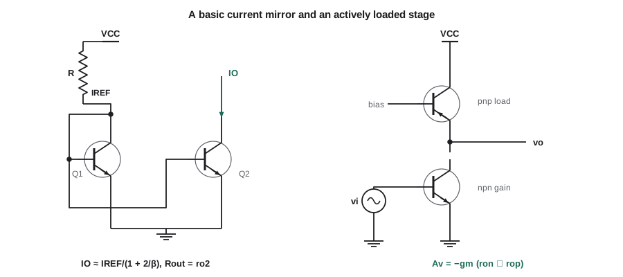
The output resistance matters as much as the current. An ideal current source has infinite output resistance; Q2 has its Early-effect resistance r_o2 = V_A/I_O, so its current rises slightly with its collector voltage. When the two collector voltages differ, the copy is in error even with infinite β, because Q1 sits at V_CE = V_BE while Q2 sits wherever the output node is:
Worked problem
Designing and checking a 1 mA mirror
Amara needs about 1 mA from a 12 V supply using transistors with β = 150, V_BE = 0.65 V and V_A = 100 V. The output transistor will sit near V_CE = 6 V. Choose R, then estimate the output current and output resistance.
Show solution
- \[R = \frac{12 - 0.65}{1\ \text{mA}} = 11.35\ \text{k}\Omega \to 11.3\ \text{k}\Omega \;(I_{REF} = 1.004\ \text{mA})\]
- Base-current error:
- \[\frac{1}{1 + 2/150} = 0.987\]
- Early-effect error:
- \[\frac{1 + 6/100}{1 + 0.65/100} = 1.053\]
- \[I_O \approx 1.004 \times 0.987 \times 1.053 \approx 1.04\ \text{mA} \qquad R_{out} \approx \frac{100}{1.04\ \text{mA}} \approx 96\ \text{k}\Omega\]
Answer: The mirror delivers about 1.04 mA, 4 percent above the reference, with an output resistance near 96 kΩ. Leo's bench measurement agrees: the output current rose from 1.00 mA at V_CE = 2 V to 1.10 mA at 12 V, which is a change of 0.1 mA for 10 V, or about 100 kΩ.
Improved mirrors
Three refinements fix the basic mirror's errors. The beta-helper mirror adds an emitter follower that supplies the two base currents, so the reference loses only the follower's base current and the error falls from 2/β to about 2/β². The Wilson mirror adds a third transistor in a local feedback loop that both cancels the base-current error to second order and raises the output resistance to about βr_o/2. The cascode mirror stacks a second mirror on the first so that the output transistor's collector voltage is held nearly constant, raising the output resistance to about βr_o for BJTs and g_m r_o² for MOSFETs. The cost is headroom: each stacked transistor needs its own V_BE or V_CE(sat), so a cascode mirror needs about 1 V more across it before it stops behaving as a current source.
| Mirror | Current error from β | Output resistance | Minimum output voltage (BJT) |
|---|---|---|---|
| Basic | ≈ 2/β | r_o | ≈ V_CE(sat), about 0.2 V |
| Beta helper | ≈ 2/β² | r_o | ≈ V_CE(sat) |
| Wilson | ≈ 2/β² | ≈ βr_o/2 | ≈ V_BE + V_CE(sat), about 0.9 V |
| Cascode | ≈ 4/β | ≈ βr_o | ≈ V_BE + V_CE(sat), about 0.9 V |
| Widlar (with R_E) | ≈ 1/β | ≈ r_o(1 + g_m R_E') | ≈ V_CE(sat) + I_O R_E |
The Widlar source for small currents
Op amp input stages often run at 10 to 20 µA. A basic mirror from a 12 V supply would need a reference resistor near 1 MΩ, which wastes chip area and is hard to make accurately. The Widlar current source solves the problem by adding a small emitter resistor R_E to the output transistor only. Now the two transistors have different V_BE, and since collector current is exponential in V_BE, a small voltage difference gives a large current ratio:
Worked problem
A 10 µA Widlar source
With I_REF = 1 mA from the 11.3 kΩ resistor, design a Widlar source for I_O = 10 µA at room temperature (V_T = 25.85 mV).
Show solution
- \[R_E = \frac{0.02585}{10 \times 10^{-6}} \ln\frac{1\ \text{mA}}{10\ \mu\text{A}} = 2585 \times 4.605 \approx 11.9\ \text{k}\Omega\]
- Output resistance with emitter degeneration (g_m = I_O/V_T = 0.387 mS, r_o = 100 V/10 µA = 10 MΩ):
- \[R_{out} \approx r_o (1 + g_m R_E) = 10\ \text{M} \times (1 + 0.387 \times 11.9) \approx 56\ \text{M}\Omega\]
Answer: Two resistors totalling about 23 kΩ set a 10 µA current, instead of the 1.1 MΩ a basic mirror would need, and the emitter degeneration raises the output resistance to tens of megohms. The current depends on V_T, which is proportional to absolute temperature, so it rises about 0.3 percent per kelvin; in an op amp input stage that drift is acceptable or even useful, because it keeps the stage's g_m nearly constant.
MOSFET mirrors
A MOSFET mirror works the same way, with two advantages: the gates draw no current, so there is no β error, and the current ratio is set by the transistors' aspect ratios W/L, which a chip designer can choose freely. In saturation the copy is
Channel-length modulation, the MOSFET's version of the Early effect, plays the role of V_A: λ is larger for short channels, so analog designers use longer-than-minimum channel lengths in mirrors to raise r_o. The mirror's output transistor stays in saturation only while V_DS ≥ V_ov, the overdrive voltage V_GS − V_t; cascode MOSFET mirrors need about 2V_ov plus a threshold, and the wide-swing cascode variants reduce that to about 2V_ov, which matters on 3.3 V and lower supplies.
Matching and layout
A mirror is only as good as the match between its transistors. For BJTs, the collector current depends exponentially on V_BE, so a V_BE mismatch of ΔV_BE gives a current error of about ΔV_BE/V_T: only 1 mV of mismatch gives nearly 4 percent. Discrete designs therefore use dual transistors in one package, or add equal emitter resistors to both transistors so that a few hundred millivolts across the resistors swamps the V_BE difference; with 100 mV across each emitter resistor, a 1 mV mismatch causes only about 1 percent error. In integrated circuits, matched devices are placed close together, oriented the same way and arranged in common-centroid patterns so that gradients in temperature and doping across the chip affect both equally. Multiple outputs at different currents come from scaling: a transistor with twice the emitter area, or twice the W/L, carries twice the current.
Active loads
A common-emitter stage with a resistor load has a voltage gain limited by the DC voltage the resistor can drop. Since g_m = I_C/V_T,
so with 6 V across R_C the gain cannot exceed about 6/0.02585 ≈ 232, however the resistor and current are chosen. Replacing R_C by a pnp current source removes the limit, because a current source has a high incremental resistance but needs only a few tenths of a volt across it. The load is then r_op, and the gain becomes
The intrinsic gain V_A/V_T is about 3,900 for a transistor with V_A = 100 V, so a single actively loaded stage can give a gain of a thousand or more. The catch is that the output node is the junction of two current sources fighting each other: any small difference between the npn's current and the pnp's current drives the output toward one rail. An actively loaded stage therefore cannot set its own DC operating point and must be placed inside a feedback loop, or paired with a differential stage whose mirror forces the currents to agree, as the next lesson shows.
import math
VT = 0.02585
# Basic mirror with base-current and Early errors
def basic(VCC, R, beta, VA, VCE2, VBE=0.65):
    iref = (VCC - VBE) / R
    io = iref / (1 + 2 / beta) * (1 + VCE2 / VA) / (1 + VBE / VA)
    return iref, io, VA / io
for vce in (2, 6, 12):
    iref, io, ro = basic(12, 11.3e3, 150, 100, vce)
    print(f"basic mirror, VCE2 = {vce:2d} V: Iref = {iref*1e3:.3f} mA, Io = {io*1e3:.3f} mA, Rout = {ro/1e3:.0f} k")
# Widlar source: solve Io*RE = VT*ln(Iref/Io) for RE given Io, then check by iteration
iref, io_target = 1e-3, 10e-6
RE = VT / io_target * math.log(iref / io_target)
io = io_target * 2
for _ in range(50):                      # fixed-point iteration on the transcendental equation
    io = VT * math.log(iref / io) / RE
print(f"Widlar: RE = {RE/1e3:.2f} k gives Io = {io*1e6:.2f} uA")
ro, gm = 100 / io, io / VT
print(f"Widlar output resistance ~ {ro*(1+gm*RE)/1e6:.0f} M (plain ro = {ro/1e6:.0f} M)")
# Active load versus resistor load at the same current
I, VAn, VAp = 0.5e-3, 100, 50
gm = I / VT
ron, rop = VAn / I, VAp / I
Aact = gm * (ron * rop / (ron + rop))
Ares = gm * (6 / I)                      # resistor dropping 6 V
print(f"gm = {gm*1e3:.2f} mS; active load gain = {Aact:.0f} ({20*math.log10(Aact):.1f} dB); 6 V resistor load gain = {Ares:.0f}")basic mirror, VCE2 = 2 V: Iref = 1.004 mA, Io = 1.005 mA, Rout = 100 k basic mirror, VCE2 = 6 V: Iref = 1.004 mA, Io = 1.044 mA, Rout = 96 k basic mirror, VCE2 = 12 V: Iref = 1.004 mA, Io = 1.103 mA, Rout = 91 k Widlar: RE = 11.90 k gives Io = 10.00 uA Widlar output resistance ~ 56 M (plain ro = 10 M) gm = 19.34 mS; active load gain = 1289 (62.2 dB); 6 V resistor load gain = 232
The output confirms the hand calculations: the basic mirror's current rises with V_CE2 exactly as Leo measured, the Widlar resistor of about 11.9 kΩ gives 10 µA, and the actively loaded stage at 0.5 mA has a gain of about 1,290, more than five times what a resistor load can give with 6 V across it. The Widlar equation has no closed-form solution for I_O when R_E is given, which is why the code iterates; designers usually do what the example did and choose I_O first, then compute R_E directly.
Reference circuits
A mirror only copies; something must set the reference. A resistor from the supply gives a current proportional to V_CC − V_BE, so the current changes with the supply, which is poor for a battery-powered or loosely regulated product. Better references make the current depend on device properties instead. A V_BE-referenced source forces V_BE across a resistor, giving I ≈ V_BE/R, nearly independent of the supply but falling about 0.3 percent per kelvin as V_BE falls about 2 mV/°C. A PTAT (proportional-to-absolute-temperature) source uses two transistors at different current densities and puts their V_BE difference, V_T ln n, across a resistor, giving a current that rises with temperature. Adding a V_BE to a scaled PTAT voltage cancels the two temperature coefficients and gives the bandgap reference, about 1.2 V, the basis of most precision voltage references and regulators. The APS-2's converter reference and its regulators already contain bandgaps, so Amara uses simple resistor references for her discrete mirrors and accepts the supply sensitivity, because the 12 V rail is regulated.
Common mistakes
MistakeAssuming a mirror copies its reference exactly.
InsteadInclude the base-current error 2/β and the Early-effect error from unequal V_CE.
MistakeTreating a BJT mirror's output as a current source down to 0 V.
InsteadIt works only while the output transistor stays out of saturation; a cascode needs about 1 V.
MistakeUsing an actively loaded stage without feedback.
InsteadIts DC operating point is set by a tiny current difference; feedback or a mirror must fix it.
MistakeBuilding a discrete mirror from two unrelated transistors.
InsteadUse a matched pair or emitter resistors; 1 mV of V_BE mismatch gives about 4 percent error.
Summary and key terms
- A current mirror copies a reference current into one or more matched transistors.
- The basic BJT mirror has a 2/β current error and output resistance r_o = V_A/I_O.
- Beta-helper, Wilson and cascode mirrors reduce errors or raise output resistance at the cost of headroom.
- The Widlar source sets small currents with small resistors: I_O R_E = V_T ln(I_REF/I_O).
- MOSFET mirrors scale current with W/L and have no gate-current error; λ sets their output resistance.
- An active load raises a stage's gain toward the intrinsic gain g_m r_o = V_A/V_T but needs feedback to set its operating point.
- References based on V_BE, PTAT voltages or a bandgap make bias currents independent of the supply.
- Current mirror
- A circuit in which a diode-connected transistor sets a voltage that makes matched transistors copy a reference current.
- Output resistance
- The incremental resistance of a current source, ΔV/ΔI at its output.
- Widlar current source
- A mirror with an emitter resistor in the output transistor, used to produce small currents.
- Wilson mirror
- A three-transistor mirror with local feedback that reduces base-current error and raises output resistance.
- Active load
- A current source used in place of a load resistor to give high voltage gain.
- Intrinsic gain
- The maximum gain of a single transistor, g_m r_o, equal to V_A/V_T for a BJT.
- Bandgap reference
- A circuit that adds a V_BE and a scaled PTAT voltage to give a temperature-stable voltage near 1.2 V.
Practice problems
Work each problem on paper first, then reveal the answer to check.
A basic mirror has β = 100. By what fraction is I_O below I_REF, neglecting the Early effect?
Show answer
1/(1 + 0.02) = 0.980, about 2 percent low.
Find the output resistance of a mirror delivering 200 µA with V_A = 80 V.
Show answer
80/200 µA = 400 kΩ.
Design a Widlar source for 20 µA from a 0.5 mA reference.
Show answer
R_E = (0.02585/20 µA) ln 25 ≈ 1293 × 3.22 ≈ 4.16 kΩ.
A MOSFET mirror has (W/L)₂ = 4(W/L)₁ and I_REF = 50 µA. Find I_O, neglecting λ.
Show answer
200 µA.
What is the maximum voltage gain of a CE stage whose load resistor drops 3 V?
Show answer
3/0.02585 ≈ 116.
An actively loaded stage runs at 1 mA with V_An = 120 V and V_Ap = 60 V. Find its gain.
Show answer
g_m = 38.7 mS; r_on ∥ r_op = 120 k ∥ 60 k = 40 kΩ; gain ≈ 1,550.
Lesson quiz · 5 questions
Score 60% or more to complete this lesson.
Create a free account to save your progress, take quizzes and earn a certificate.