
PHYS-410 · Lesson 10 of 12 · 21 min
Semiconductors: carriers, doping, p–n junctions and devices
Semiconductors are the materials whose band gaps are small enough that their electrical properties can be controlled: by temperature, by light, by electric fields and above all by adding tiny, precisely chosen amounts of impurities. That controllability made possible the transistor, the integrated circuit, the light-emitting diode, the solar cell and the laser diode. This lesson applies the band theory of lessons 8 and 9 to semiconductors. It calculates how many carriers a pure semiconductor has, how doping changes that number by many orders of magnitude, and how a junction between differently doped regions produces the one-way flow of current that underlies nearly all of electronics.
Intrinsic carriers
In a pure, or intrinsic, semiconductor at absolute zero, the valence band is full and the conduction band empty. At temperature \(T\), some electrons are thermally excited across the gap \(E_g\), leaving an equal number of holes. Near the bottom of the conduction band, at energy \(E_c\), electrons behave as free particles with effective mass \(m_e^*\); near the top of the valence band, at \(E_v\), holes behave as free particles with mass \(m_h^*\). Because the gap is much larger than \(k_BT\), the Fermi–Dirac occupation of the conduction band reduces to a Boltzmann factor, and integrating over the parabolic density of states gives
where \(\mu\) is the chemical potential, conventionally called the Fermi level, and \(N_c\) and \(N_v\) are the effective densities of states, about \(10^{19}\ \text{cm}^{-3}\) at room temperature. Multiplying the two gives the law of mass action,
which holds whether or not the crystal is doped, as long as the Fermi level is well inside the gap. In an intrinsic crystal, \(n = p = n_i\), and the Fermi level sits near the middle of the gap, shifted slightly toward the band with the lighter carriers. The intrinsic density depends exponentially on \(E_g/2k_BT\), so small differences in the gap make enormous differences in conductivity. The program evaluates \(n_i\) for silicon, germanium and gallium arsenide, including the slow decrease of each gap with temperature.
import math
# Carriers in semiconductors: intrinsic density, doping and freeze-out, and the p-n junction.
kB = 8.617333e-5      # eV/K
mats = {  # Nc, Nv at 300 K (per cm^3), Varshni Eg(0), alpha (eV/K), beta (K)
    'Si':   (2.86e19, 3.10e19, 1.170, 4.73e-4, 636),
    'Ge':   (1.04e19, 6.0e18, 0.7437, 4.77e-4, 235),
    'GaAs': (4.7e17, 7.0e18, 1.519, 5.41e-4, 204),
}
def Eg(m, T): _, _, E0, al, be = mats[m]; return E0 - al * T * T / (T + be)
def ni(m, T):
    Nc, Nv = mats[m][:2]
    s = (T / 300) ** 1.5
    return math.sqrt(Nc * s * Nv * s) * math.exp(-Eg(m, T) / (2 * kB * T))
print("intrinsic carrier density n_i (per cm^3)")
print("   T (K)        Si          Ge         GaAs")
for T in (200, 300, 400, 500):
    print(f"   {T:4d}  " + "  ".join(f"{ni(m, T):10.2e}" for m in mats))
print(f"   band gaps at 300 K: " + ", ".join(f"{m} {Eg(m, 300):.3f} eV" for m in mats))
print()
# n-type silicon with Nd = 1e16 phosphorus donors, Ed = 0.045 eV below the conduction band
Nd, Ed = 1e16, 0.045
def n_electrons(T):
    Nc, Nv = mats['Si'][0] * (T / 300) ** 1.5, mats['Si'][1] * (T / 300) ** 1.5
    lo, hi = -1.5, 0.2                       # Fermi level relative to the conduction band edge, eV
    for _ in range(200):
        mu = (lo + hi) / 2
        n = Nc * math.exp(mu / (kB * T))
        p = Nv * math.exp((-Eg('Si', T) - mu) / (kB * T))
        Nd_plus = Nd / (1 + 2 * math.exp((mu + Ed) / (kB * T)))
        if n - p - Nd_plus > 0: hi = mu
        else: lo = mu
    return n
print("n-type Si, Nd = 1e16 per cm^3: electron density n(T)")
for T in (30, 50, 100, 200, 300, 500, 700):
    n = n_electrons(T)
    print(f"   T = {T:3d} K: n = {n:9.2e}  (n/Nd = {n / Nd:6.3f}, n_i = {ni('Si', T):9.2e})")
print()
# Silicon p-n junction and the ideal diode law
NA, ND = 1e17, 1e16
Vbi = kB * 300 * math.log(NA * ND / ni('Si', 300) ** 2)
print(f"Si junction NA = 1e17, ND = 1e16: built-in potential = {Vbi:.3f} V")
eps = 11.7 * 8.854e-14   # F/cm
W = math.sqrt(2 * eps * Vbi / 1.602e-19 * (1 / NA + 1 / ND))
print(f"depletion width at zero bias = {W * 1e4:.3f} um")
I0 = 1e-12
for V in (-1.0, -0.1, 0.0, 0.3, 0.5, 0.6, 0.7):
    I = I0 * (math.exp(V / (kB * 300)) - 1)
print(f" V = {V:+.1f} V: I = {I:+.3e} A")intrinsic carrier density n_i (per cm^3)
T (K) Si Ge GaAs
200 5.67e+04 6.54e+09 3.39e-01
300 1.07e+10 2.11e+13 2.05e+06
400 5.63e+12 1.44e+15 6.02e+09
500 2.72e+14 2.00e+16 8.02e+11
band gaps at 300 K: Si 1.125 eV, Ge 0.663 eV, GaAs 1.422 eV
n-type Si, Nd = 1e16 per cm^3: electron density n(T)
T = 30 K: n = 1.12e+13 (n/Nd = 0.001, n_i = 5.65e-81)
T = 50 K: n = 5.18e+14 (n/Nd = 0.052, n_i = 2.68e-41)
T = 100 K: n = 6.85e+15 (n/Nd = 0.685, n_i = 2.74e-11)
T = 200 K: n = 9.83e+15 (n/Nd = 0.983, n_i = 5.67e+04)
T = 300 K: n = 9.96e+15 (n/Nd = 0.996, n_i = 1.07e+10)
T = 500 K: n = 1.00e+16 (n/Nd = 1.000, n_i = 2.72e+14)
T = 700 K: n = 3.29e+16 (n/Nd = 3.289, n_i = 2.74e+16)
Si junction NA = 1e17, ND = 1e16: built-in potential = 0.770 V
depletion width at zero bias = 0.331 um
V = -1.0 V: I = -1.000e-12 A
V = -0.1 V: I = -9.791e-13 A
V = +0.0 V: I = +0.000e+00 A
V = +0.3 V: I = +1.096e-07 A
V = +0.5 V: I = +2.510e-04 A
V = +0.6 V: I = +1.201e-02 A
V = +0.7 V: I = +5.748e-01 AAt 300 K, silicon has \(n_i \approx 1.1 \times 10^{10}\ \text{cm}^{-3}\), germanium \(2 \times 10^{13}\) and gallium arsenide only \(2 \times 10^6\). With about \(5 \times 10^{22}\) atoms per cubic centimeter, intrinsic silicon has one free electron for every 5 trillion atoms. Heating silicon from 300 K to 400 K raises \(n_i\) about 500-fold, which is why silicon devices stop working well above about 450 K, while wide-gap materials such as silicon carbide (3.3 eV) and gallium nitride (3.4 eV) operate at higher temperatures and voltages in electric-vehicle chargers and power supplies.
Doping
Replace one silicon atom in a million by a phosphorus atom. Phosphorus has five valence electrons; four form bonds with the neighboring silicon atoms, and the fifth is left over. It is bound to the \(\text{P}^+\) ion by the Coulomb attraction, screened by the silicon's dielectric constant \(\varepsilon_r = 11.7\), and it moves with the conduction-band effective mass. This is a hydrogen atom with rescaled parameters. Its binding energy is the Rydberg energy times \(m^*/(m\varepsilon_r^2)\), and its radius the Bohr radius times \(\varepsilon_rm/m^*\):
The measured donor level of phosphorus in silicon is 45 meV below the conduction band. Because this is less than twice \(k_BT\) at room temperature, nearly every donor is ionized, contributing one electron to the conduction band. The orbit spans several hundred atoms, which justifies treating the silicon as a continuous medium. Such impurities are donors, and silicon doped with them is n-type, with electrons as the majority carriers. Group III atoms such as boron, with three valence electrons, accept an electron from the valence band, creating a hole bound to the \(\text{B}^-\) ion with a similar small binding energy: they are acceptors, and the material is p-type.
In n-type material with donor density \(N_d \gg n_i\), the electron density is \(n \approx N_d\), and by mass action the hole density is \(p = n_i^2/N_d\). A doping of \(10^{16}\ \text{cm}^{-3}\), one atom in five million, raises the electron density a million-fold and lowers the hole density to about \(10^4\ \text{cm}^{-3}\). The conductivity, \(\sigma = ne\mu_e + pe\mu_h\), where \(\mu_e\) and \(\mu_h\) are the mobilities (about 1400 and 450 \(\text{cm}^2\) per volt-second in lightly doped silicon), rises by the same factor.
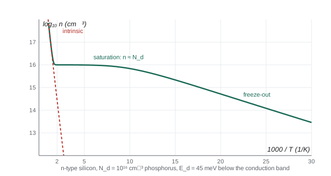
The program solves the full charge-neutrality condition, \(n = p + N_d^+\), for the Fermi level at each temperature, including the fraction of donors that keep their electron. Three regimes appear. Below about 100 K, electrons fall back onto the donors: this is freeze-out, and at 30 K only one donor in a thousand is ionized. From about 150 to 500 K, essentially all donors are ionized and \(n \approx N_d\), independent of temperature: the saturation range in which silicon devices are designed to operate. Above about 600 K, \(n_i\) exceeds \(N_d\), and the material becomes intrinsic; by 700 K the electron density is more than three times the donor density. Semiconductor engineers choose doping levels so that the operating temperature range lies well within saturation.
The p–n junction
The most important structure in electronics is the junction between p-type and n-type regions of the same crystal. Before contact, the Fermi level is near the conduction band on the n side and near the valence band on the p side. When they are joined, electrons diffuse from the n side, where they are plentiful, into the p side, and holes diffuse the other way. They leave behind uncompensated ionized donors (positive) on the n side and ionized acceptors (negative) on the p side, a region depleted of mobile carriers, the depletion region. The charges create an electric field that opposes further diffusion, and equilibrium is reached when the Fermi level is the same everywhere. The bands bend by the built-in potential
which the program finds to be 0.77 V for silicon with \(N_a = 10^{17}\) and \(N_d = 10^{16}\ \text{cm}^{-3}\). Solving Poisson's equation for the uniform space charge gives the depletion width \(W = \sqrt{2\varepsilon V_{bi}(1/N_a + 1/N_d)/e}\), about 0.33 µm here, lying mostly on the more lightly doped side.
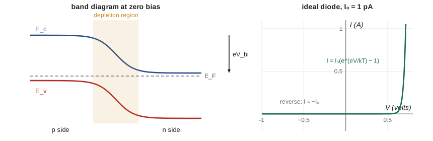
Now apply a voltage \(V\), positive on the p side (forward bias). The barrier falls to \(e(V_{bi} - V)\), and the number of majority carriers able to diffuse across rises by \(e^{eV/k_BT}\). Under reverse bias the barrier rises and only the small flow of thermally generated minority carriers remains. William Shockley derived the result in 1949:
the ideal diode equation. The saturation current \(I_0\), proportional to \(n_i^2\), is tiny for silicon, so with \(I_0 = 1\) pA the program shows the current rising from 0.1 µA at 0.3 V to 0.57 A at 0.7 V, a factor of 10 for every 60 mV. Under reverse bias, the current stays at \(-I_0\) until breakdown. This rectifying behavior is the basis of diodes; a junction lit by photons with energy above the gap generates electron–hole pairs that the built-in field separates, which is how a solar cell works; and in a direct-gap semiconductor such as gallium arsenide or gallium nitride, electrons and holes injected by forward bias recombine and emit light, which is how an LED works. Shuji Nakamura, Isamu Akasaki and Hiroshi Amano shared the 2014 Nobel Prize in Physics for the efficient blue LED in gallium nitride.
Transistors and integrated circuits
The bipolar junction transistor, invented at Bell Laboratories in 1947–48 by Bardeen, Brattain and Shockley, uses two junctions back to back: a small current into the thin middle region controls a much larger current through the device. Modern integrated circuits use instead the metal–oxide–semiconductor field-effect transistor, or MOSFET, in which a voltage on a gate electrode, insulated from the silicon by a thin oxide, attracts carriers to form a conducting channel between two doped regions. Integrated circuits now contain tens of billions of transistors on a chip, with critical features a few tens of nanometers across. At those sizes, quantum tunneling through the gate oxide and the statistics of individual dopant atoms are design constraints, so the physics of this course is part of daily engineering practice.
Worked problem
Doped silicon
Silicon at 300 K is doped with \(N_a = 10^{17}\ \text{cm}^{-3}\) boron acceptors. With \(n_i = 1.07 \times 10^{10}\ \text{cm}^{-3}\), find the hole and electron densities and the position of the Fermi level relative to the valence band, using \(N_v = 3.1 \times 10^{19}\ \text{cm}^{-3}\).
Show solution
- All acceptors are ionized: \(p \approx 10^{17}\ \text{cm}^{-3}\).
- \(n = n_i^2/p = (1.07 \times 10^{10})^2/10^{17} = 1.1 \times 10^3\ \text{cm}^{-3}\).
- \(\mu - E_v = k_BT\ln(N_v/p) = 0.02585 \times \ln(310) = 0.148\) eV.
Answer: \(p = 10^{17}\), \(n \approx 1100\ \text{cm}^{-3}\), and the Fermi level lies about 0.15 eV above the valence band.
Common mistakes
MistakeExpecting \(np = n_i^2\) to fail in doped material.
InsteadMass action holds for doped and undoped crystals alike, as long as \(\mu\) is well inside the gap.
MistakeUsing the atomic binding energy for a donor.
InsteadThe dielectric constant and effective mass reduce it to tens of meV.
MistakeAssuming carrier density always rises with temperature in a doped semiconductor.
InsteadIn saturation it is flat at \(N_d\).
MistakePlacing the depletion region mostly on the heavily doped side.
InsteadIt extends mainly into the lightly doped side, to balance the charge.
MistakeForgetting the \(-1\) in the diode equation.
InsteadWithout it the current would not vanish at \(V = 0\).
Summary and key terms
- \(n = N_ce^{-(E_c - \mu)/k_BT}\), \(p = N_ve^{-(\mu - E_v)/k_BT}\) and \(np = n_i^2 = N_cN_ve^{-E_g/k_BT}\); silicon has \(n_i \approx 10^{10}\ \text{cm}^{-3}\) at 300 K.
- Donors and acceptors are hydrogen-like impurities with binding energies of tens of meV; they make n-type and p-type material.
- Doped silicon shows freeze-out, saturation \(n \approx N_d\), and intrinsic behavior as temperature rises.
- A p–n junction has a built-in potential \(eV_{bi} = k_BT\ln(N_aN_d/n_i^2)\) across a depletion region.
- The ideal diode obeys \(I = I_0(e^{eV/k_BT} - 1)\); junctions underlie diodes, solar cells, LEDs and transistors.
- Intrinsic semiconductor
- A pure semiconductor with \(n = p = n_i\).
- Donor
- An impurity that gives an electron to the conduction band.
- Acceptor
- An impurity that takes an electron from the valence band, creating a hole.
- Law of mass action
- \(np = n_i^2\) in thermal equilibrium.
- Depletion region
- The region at a junction emptied of mobile carriers, containing fixed ionized dopants.
Practice problems
Work each problem on paper first, then reveal the answer to check.
By what factor does \(n_i\) in silicon change between 300 K and 400 K, according to the program?
Show answer
From \(1.07 \times 10^{10}\) to \(5.6 \times 10^{12}\), about 500 times.
Estimate the donor binding energy in germanium, with \(m^* = 0.12m\) and \(\varepsilon_r = 16\).
Show answer
\(13.6 \times 0.12/256 = 6.4\) meV.
n-type silicon has \(N_d = 10^{15}\ \text{cm}^{-3}\). Find \(p\) at 300 K.
Show answer
\(p = n_i^2/N_d \approx 1.1 \times 10^5\ \text{cm}^{-3}\).
How much forward voltage increases the diode current tenfold at 300 K?
Show answer
\(k_BT\ln10/e = 59.5\) mV.
Why is silicon carbide preferred for high-temperature power electronics?
Show answer
Its 3.3 eV gap keeps \(n_i\) small at high temperature, so the doping still controls conduction.
Lesson quiz · 5 questions
Score 60% or more to complete this lesson.
Create a free account to save your progress, take quizzes and earn a certificate.