
ELE-455 · Lesson 5 of 12 · 24 min
Low-noise amplifiers
The cabinet receiver chosen in lesson 1 puts a low-noise amplifier (LNA) between the SAW filter and the transceiver. Its job is easy to state: provide about 15 dB of gain with a noise figure near 1 dB, enough linearity not to become the weak link, and an input that the SAW filter sees as a reasonable 50 Ω load. It must also be stable, never oscillating with any antenna, filter or cable that might be connected to it. Priya has found a low-cost silicon-germanium transistor with a data sheet that gives S-parameters and noise parameters at 3 V and 10 mA, and this lesson follows her design from those data to a matched, stable amplifier. Integrated LNA chips are also available, and Amara keeps one as a fall-back, but designing a discrete LNA shows what every LNA designer, on a board or inside a chip, has to balance.
Noise parameters
A transistor's noise figure depends on the impedance of the source driving it. Four noise parameters describe this dependence completely: the minimum noise figure F_min, the source reflection coefficient Γ_opt that achieves it, and the noise resistance R_n, which sets how quickly the noise figure rises as the source moves away from Γ_opt.
For Priya's transistor at 915 MHz the data sheet gives F_min = 0.60 dB, Γ_opt = 0.45 at 40° and R_n = 8 Ω. A small R_n is good news: the noise figure is not very sensitive to the source impedance, so a compromise between noise and other goals costs little. Note that Γ_opt is not the conjugate of the transistor's input reflection coefficient S₁₁*. The source impedance that gives the least noise is set by the correlation between the transistor's internal noise sources, not by power transfer, and in general a noise match and a power match are different. That single fact shapes the whole LNA design.
The set of source reflection coefficients that give a particular noise figure F_i forms a circle on the Smith chart, a noise circle. With N = (F_i − F_min)|1 + Γ_opt|²/(4R_n/Z₀), the circle has its center at Γ_opt/(N + 1) and radius √(N(N + 1 − |Γ_opt|²))/(N + 1). Any source impedance inside the 1.0 dB circle keeps the transistor's own noise figure below 1.0 dB.
Stability
A transistor with feedback from output to input, through S₁₂, can oscillate if the impedances at its ports are unfavorable. It does so when the reflection coefficient looking into one port has magnitude greater than one, meaning the port returns more power than it receives. An amplifier is unconditionally stable if no passive source or load, anywhere inside the Smith chart, can make that happen; otherwise it is potentially unstable, and the designer must keep the source and load away from the dangerous regions. The Rollett stability factor K and the determinant Δ test this.
The amplifier is unconditionally stable if K > 1 and |Δ| < 1. The single-parameter test μ > 1, where μ = (1 − |S₁₁|²)/(|S₂₂ − ΔS₁₁*| + |S₁₂S₂₁|), says the same thing in one number and also measures how far from instability the device is. The boundaries of the unstable regions are the stability circles: the input stability circle is the set of source reflection coefficients for which |Γ_out| = 1, and the output circle the set of load coefficients for which |Γ_in| = 1.
Stability must hold at all frequencies, not just in the band. A transistor with plenty of gain at low frequencies and feedback that becomes larger as frequency rises may be stable at 915 MHz and oscillate at 3 GHz, or at 100 MHz where the bias network presents an unexpected impedance. Priya checks K and μ from 10 MHz to 6 GHz using the data sheet's full S-parameter file, and Leo will look for oscillation on a spectrum analyzer with the input open, shorted and terminated.
import cmath, math

# LNA transistor at 915 MHz, 3 V, 10 mA (illustrative datasheet values)
def P(m, deg): return cmath.rect(m, math.radians(deg))
Z0 = 50.0
T = {'S11': P(0.65, -80), 'S21': P(6.5, 110), 'S12': P(0.06, 50), 'S22': P(0.45, -40)}
Fmin_db, Gopt, Rn = 0.60, P(0.45, 40), 8.0      # noise parameters, Rn in ohms

def stability(S):
    S11, S21, S12, S22 = S['S11'], S['S21'], S['S12'], S['S22']
    D = S11*S22 - S12*S21
    K = (1 - abs(S11)**2 - abs(S22)**2 + abs(D)**2)/(2*abs(S12*S21))
    mu = (1 - abs(S11)**2)/(abs(S22 - D*S11.conjugate()) + abs(S12*S21))
    return D, K, mu

def add_shunt_out(S, R):
    """Cascade a shunt resistor R at the output port (via ABCD parameters)."""
    s11, s12, s21, s22 = S['S11'], S['S12'], S['S21'], S['S22']
    A = ((1+s11)*(1-s22) + s12*s21)/(2*s21); B = Z0*((1+s11)*(1+s22) - s12*s21)/(2*s21)
    C = ((1-s11)*(1-s22) - s12*s21)/(2*s21*Z0); Dd = ((1-s11)*(1+s22) + s12*s21)/(2*s21)
    C = C + A/R; Dd = Dd + B/R
    den = A + B/Z0 + C*Z0 + Dd
    return {'S11': (A + B/Z0 - C*Z0 - Dd)/den, 'S12': 2*(A*Dd - B*C)/den, 'S21': 2/den, 'S22': (-A + B/Z0 - C*Z0 + Dd)/den}

D, K, mu = stability(T)
print(f"bare transistor: |Delta| {abs(D):.3f}  K {K:.3f}  mu {mu:.3f}  (K < 1: potentially unstable)")
print(f"  maximum stable gain |S21/S12| = {10*math.log10(abs(T['S21'])/abs(T['S12'])):.1f} dB")
for R in (1000, 330, 150, 120):
    D, K, mu = stability(add_shunt_out(T, R))
    print(f"  with {R:4d} ohm shunt at the output: K {K:.3f}  mu {mu:.3f}")

S = add_shunt_out(T, 120)
S11, S21, S12, S22 = S['S11'], S['S21'], S['S12'], S['S22']
D, K, mu = stability(S)
mag = 10*math.log10(abs(S21)/abs(S12)*(K - math.sqrt(K*K - 1)))
print(f"stabilized: K {K:.3f}, maximum available gain {mag:.1f} dB")

def nf(Gs):
    F = 10**(Fmin_db/10) + 4*Rn/Z0*abs(Gs - Gopt)**2/((1 - abs(Gs)**2)*abs(1 + Gopt)**2)
    return 10*math.log10(F)
def gout(Gs): return S22 + S12*S21*Gs/(1 - S11*Gs)
def gin(GL): return S11 + S12*S21*GL/(1 - S22*GL)
def gt(Gs, GL):
    return 10*math.log10((1 - abs(Gs)**2)*abs(S21)**2*(1 - abs(GL)**2)/(abs(1 - Gs*gin(GL))**2*abs(1 - S22*GL)**2))
# simultaneous conjugate match (exists because K > 1)
B1 = 1 + abs(S11)**2 - abs(S22)**2 - abs(D)**2; C1 = S11 - D*S22.conjugate()
Gms = (B1 - math.sqrt(B1*B1 - 4*abs(C1)**2))/(2*C1)
for name, Gs in (("noise match  Gs = Gopt", Gopt), ("gain match   Gs = Gms ", Gms)):
    GL = gout(Gs).conjugate()
    Gi = gin(GL); m = abs((Gi - Gs.conjugate())/(1 - Gi*Gs))
    rl = f"{-20*math.log10(m):5.1f} dB" if m > 1e-4 else "matched"
    print(f"{name}  NF {nf(Gs):4.2f} dB  gain {gt(Gs, GL):5.1f} dB  input return loss {rl}")

# 1.0 dB noise circle
Fi = 10**(1.0/10); Fm = 10**(Fmin_db/10)
N = (Fi - Fm)/(4*Rn/Z0)*abs(1 + Gopt)**2
cf = Gopt/(N + 1); rf = math.sqrt(N*(N + 1 - abs(Gopt)**2))/(N + 1)
print(f"1.0 dB noise circle: middle point {abs(cf):.3f} at {math.degrees(cmath.phase(cf)):.0f} deg, radius {rf:.3f}")
print(f"Gms lies {abs(Gms - cf):.3f} from that middle point -> {'inside' if abs(Gms - cf) < rf else 'outside'} the 1.0 dB circle")bare transistor: |Delta| 0.445 K 0.735 mu 0.737 (K < 1: potentially unstable) maximum stable gain |S21/S12| = 20.3 dB with 1000 ohm shunt at the output: K 0.791 mu 0.810 with 330 ohm shunt at the output: K 0.904 mu 0.926 with 150 ohm shunt at the output: K 1.107 mu 1.063 with 120 ohm shunt at the output: K 1.201 mu 1.106 stabilized: K 1.201, maximum available gain 17.6 dB noise match Gs = Gopt NF 0.60 dB gain 15.2 dB input return loss 4.5 dB gain match Gs = Gms NF 1.54 dB gain 17.6 dB input return loss matched 1.0 dB noise circle: middle point 0.339 at 40 deg, radius 0.457 Gms lies 0.647 from that middle point -> outside the 1.0 dB circle
Stabilizing the transistor
The program shows that the bare transistor is potentially unstable at 915 MHz: K = 0.735 and μ = 0.737. Its maximum stable gain |S₂₁/S₁₂| is 20.3 dB, the most it could deliver with matching networks right at the edge of oscillation. The input stability circle lies mostly outside the Smith chart, but a slice of it intrudes into the upper part of the chart, a region of source impedances that would make the device oscillate.
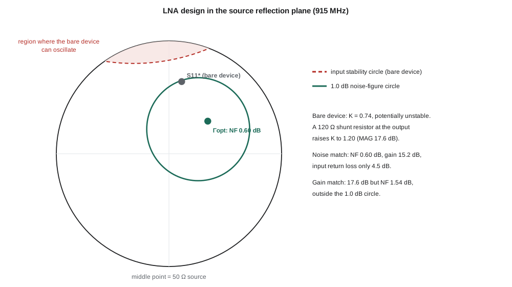
Designers stabilize transistors by adding loss where it costs the least. A resistor at the input adds noise directly and is avoided. A resistor at the output, in shunt or series, adds noise only after the transistor's gain, so its effect on the noise figure is small. Inductive emitter degeneration, a small inductance in series with the emitter, is another common technique: it reduces gain, improves stability and moves Γ_opt toward S₁₁*, bringing the noise and power matches closer together. Priya tries a shunt resistor at the output first because it is easy to evaluate: the program cascades it with the transistor and recomputes K. A 1 kΩ resistor raises K only to 0.79; 150 Ω gives 1.11; 120 Ω gives 1.20, and Priya adopts it. The price is gain: the maximum available gain, which now exists because the device is unconditionally stable, is 17.6 dB, below the 20.3 dB maximum stable gain of the bare device. The resistor's noise, divided by the transistor's gain, adds only a few hundredths of a decibel and is neglected here; the final simulation includes it.
Noise match, gain match and the compromise
With the stabilized device, two choices of source impedance stand out. A noise match, Γ_s = Γ_opt, gives the minimum noise figure of 0.60 dB and a transducer gain of 15.2 dB when the output is conjugately matched. A simultaneous conjugate match, possible now that K > 1, gives the maximum available gain of 17.6 dB and a perfect input match, but a noise figure of 1.54 dB, because its source point lies 0.65 away from the center of the 1.0 dB circle, well outside it.
For the cabinet receiver the noise figure matters most, and 15 dB of gain is enough to make the transceiver's 5 dB noise figure a small contribution. The noise match has one serious drawback, however: the input return loss is only 4.5 dB. The SAW filter in front of the LNA was designed to work between 50 Ω terminations; terminated in a poor match its passband ripples and its skirts change, and the filter's own loss rises. Priya has three options. She can move the source point from Γ_opt partway toward the simultaneous-match point, trading a few tenths of a decibel of noise figure for better return loss; the 1.0 dB circle shows how far she can go. She can add inductive emitter degeneration so that the noise and power matches coincide more closely, the standard technique in integrated LNAs. Or she can use a balanced amplifier, two identical LNAs between 90° hybrid couplers, in which reflections from the two devices cancel at the input port, giving a good return loss with a noise match at the cost of twice the parts and current.
Priya chooses emitter degeneration with a 0.6 nH inductance, realized mostly by the emitter vias and a short trace. In her simulation it brings the input return loss at Γ_opt to 11 dB with the noise figure rising to 0.75 dB, a good compromise. The SAW filter's data sheet shows that it tolerates a 10 dB return loss on its output with little change.
Worked problem
A point on the noise-figure equation
The source is the 50 Ω center of the chart, Γ_s = 0. Find the transistor's noise figure with F_min = 0.60 dB, Γ_opt = 0.45 at 40° and R_n = 8 Ω.
Show solution
- \[F_{min} = 10^{0.06} = 1.148\]
- \[|1 + \Gamma_{opt}|^2 = |1 + 0.345 + j0.289|^2 = 1.809 + 0.084 = 1.893\]
- \[F = 1.148 + \frac{4(8)}{50}\cdot\frac{0.45^2}{1 \times 1.893} = 1.148 + 0.068 = 1.216\]
- \[\mathrm{NF} = 10\log_{10}(1.216) = 0.85\ \text{dB}\]
Answer: About 0.85 dB, showing how gently this device's noise figure rises away from Γ_opt.
Linearity and bias
An LNA must also handle strong signals. Its IIP3 and 1 dB compression point are set mainly by the bias current and supply voltage: more current gives a higher intercept, at the price of power. At 3 V and 10 mA, Priya's transistor has an output IIP3 of about +15 dBm and an input IIP3 near 0 dBm with 15 dB of gain, the value used in lesson 1's cascade. In the cabinet the supply is not a constraint, so she keeps 10 mA; a battery-powered design would run nearer 3 to 5 mA and accept the lower intercept.
The bias network must not disturb the radio-frequency circuit. Priya feeds the collector through an inductor with a high impedance at 915 MHz, bypassed on its supply side, and sets the base current with a resistor network that includes a DC feedback path from the collector, so that the operating point stays steady as the transistor's current gain changes with temperature and from part to part. At low frequencies the bias inductors and bypass capacitors present impedances that can make the transistor unstable, which is why the stability check extends to 10 MHz; a small series resistor in the base bias feed damps any low-frequency resonance.
Layout and measurement
The LNA layout follows lesson 4: grounded coplanar waveguide with many vias, the emitter grounded through short vias directly beneath the transistor, the input match as close to the base as possible, and the whole stage under a shield can shared with the SAW filter. Leo measures the finished amplifier with the VNA for gain and return loss, with a noise-figure analyzer and a calibrated noise source for noise figure, and with two signal generators combined into a spectrum analyzer for IIP3. He also repeats the stability check physically by placing a sliding short on the input, a short-circuit whose position along a line can be adjusted so that its reflection coefficient sweeps around the edge of the Smith chart, and watching for oscillation.
The first boards measure a noise figure of 0.9 dB including the input match loss, a gain of 14.7 dB, an input return loss of 10.5 dB and no oscillation with any termination. With the 1.5 dB SAW in front, the cascade noise figure is close to the 2.7 dB used in lesson 1.
Common mistakes
MistakeDesigning an LNA input for a conjugate power match.
InsteadMinimum noise requires Γ_opt, which differs from S₁₁*; designers compromise between noise and return loss.
MistakeChecking stability only in the operating band.
InsteadOscillation can occur wherever the device has gain; check K and μ from low frequencies to well above the band.
MistakeStabilizing an LNA with a resistor at its input.
InsteadInput resistance adds noise directly; output or degeneration techniques cost far less noise figure.
MistakeIgnoring how a poor LNA input match affects the filter in front of it.
InsteadFilters are designed for proper terminations; a mismatch changes their ripple, loss and rejection.
Summary and key terms
- A device's noise figure depends on the source impedance through F_min, Γ_opt and R_n; the noise match generally differs from the power match.
- Noise circles show source impedances that give a chosen noise figure.
- K > 1 with |Δ| < 1, or μ > 1, means unconditional stability; stability circles mark dangerous source and load regions.
- Output resistors and inductive degeneration stabilize a transistor with little noise penalty; degeneration also brings Γ_opt toward S₁₁*.
- A balanced amplifier gives good return loss with a noise match.
- LNA linearity is set mainly by bias current; bias networks must not create low-frequency instability.
- Low-noise amplifier (LNA)
- The first amplifier in a receiver, designed for low noise figure.
- Noise parameters
- F_min, Γ_opt and R_n, which describe a device's noise figure versus source impedance.
- Noise circle
- The set of source reflection coefficients giving a constant noise figure.
- Rollett stability factor K
- A figure computed from S-parameters that tests unconditional stability with |Δ|.
- Stability circle
- The boundary of source or load impedances at which the other port's reflection has magnitude one.
- Maximum available gain
- The gain of an unconditionally stable device with both ports conjugately matched.
- Emitter degeneration
- Impedance in series with the emitter, used to stabilize and to align noise and power matches.
- Balanced amplifier
- Two amplifiers between quadrature hybrids, giving good port matches.
Practice problems
Work each problem on paper first, then reveal the answer to check.
A device has |S₂₁| = 4 and |S₁₂| = 0.05. What is its maximum stable gain?
Show answer
10 log₁₀(4/0.05) = 19.0 dB.
A transistor has K = 1.3 and |Δ| = 0.4. Is it unconditionally stable?
Show answer
Yes.
Why does a resistor at an LNA's output cost little noise figure?
Show answer
Its noise is divided by the transistor's gain when referred to the input.
What does a small R_n tell the designer?
Show answer
The noise figure rises slowly as the source moves away from Γ_opt, so compromise matches are cheap.
Name two ways to get good input return loss with a noise-matched LNA.
Show answer
Inductive emitter or source degeneration; a balanced amplifier with hybrid couplers.
Why is the LNA stability checked down to 10 MHz?
Show answer
Bias networks and bypass parts can present impedances at low frequencies where the device has high gain.
Lesson quiz · 5 questions
Score 60% or more to complete this lesson.
Create a free account to save your progress, take quizzes and earn a certificate.