
ELE-445 · Lesson 6 of 12 · 23 min
Sequential circuits, timing and low-power design
Combinational gates compute; sequential elements remember. The CX-1 period counters, the register file and the serial interface are all synchronous logic: banks of flip-flops that capture new values on each edge of a clock, with combinational logic between them. This lesson opens up the flip-flop, defines the timing constraints that every synchronous path must meet, and then turns to the problem that matters most for CX-1: power. The pedestrian stations Cedarline wants to sell for rural crossings run from a small solar panel and battery, and every microwatt the chip saves is battery capacity that keeps the station working through a week of overcast December days.
Latches and flip-flops
A latch is a storage element that is transparent while its clock is at one level and holds its value while the clock is at the other. The standard CMOS latch uses a transmission gate to pass the input to a pair of cross-coupled inverters when the clock is high and a second transmission gate to close the inverter loop when the clock is low. The cross-coupled pair is bistable, with two stable states, and holds its value indefinitely without refreshing as long as power is applied. An edge-triggered D flip-flop is two latches in series, a master transparent while the clock is low and a slave transparent while it is high; the output changes only just after the rising edge, when the slave opens and passes what the master captured. This master-slave structure is what the standard cell library provides, typically in about twenty to twenty-four transistors, with variants that add asynchronous reset, scan inputs for test and enable inputs.
Three numbers characterize a flip-flop. The clock-to-Q delay t_cq is the time from the clock edge to a valid output. The setup time t_setup is how long before the clock edge the input must be stable for the master latch to capture it reliably. The hold time t_hold is how long after the clock edge the input must remain stable so that the master latch, closing, does not capture a new value by mistake. In the illustrative CX-1 library at the typical corner they are about 180 ps, 90 ps and 40 ps.
Timing constraints
A synchronous path starts at one flip-flop, passes through combinational logic and ends at another. Two constraints apply. The setup constraint says the data launched by one clock edge must arrive at the next flip-flop at least a setup time before the following edge. The hold constraint says the data launched by a clock edge must not arrive at the next flip-flop so quickly that it corrupts the value being captured on that same edge. Clock skew, the difference in clock arrival times at the two flip-flops, enters both. When the capturing flip-flop receives its clock later than the launching flip-flop, setup becomes easier and hold harder; the worst case for each is taken by static timing analysis.
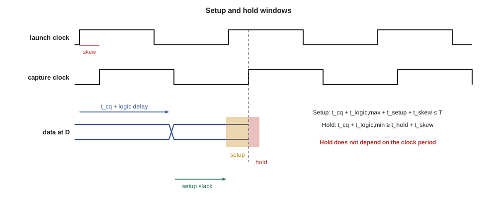
The setup constraint limits the clock frequency, and violating it is fixed by slowing the clock or speeding the logic. The hold constraint is independent of the clock frequency, and violating it cannot be fixed by slowing the clock. A chip with a hold violation fails at every frequency, so hold checks are the more dangerous of the two. Hold problems arise in short paths, such as a shift register in which one flip-flop's output goes straight to the next flip-flop's input, combined with clock skew.
Amara runs the CX-1 counter paths through the constraints with representative numbers in a short script.
# Timing and power of the CX-1 loop-counter block (illustrative numbers)
f_clk = 20e6
T = 1 / f_clk * 1e12            # ps
t_cq, t_setup, t_hold = 180, 90, 40     # flip-flop, ps, typical corner
skew = 120                      # worst clock arrival difference, ps
paths = {"24-bit counter carry": 2900, "period compare": 4100, "register file write": 3300,
         "SPI shift": 650, "short path (shift reg)": 60}
print(f"clock period {T:.0f} ps")
for name, d in paths.items():
    setup_slack = T - (t_cq + d + t_setup + skew)
    hold_slack = (t_cq + d) - (t_hold + skew)
    print(f"  {name:<24} setup slack {setup_slack:6.0f} ps   hold slack {hold_slack:5.0f} ps")
# slow corner: logic 1.6x slower; the short path then
for k, label in ((1.6, "slow corner"), (0.7, "fast corner")):
    d = paths["short path (shift reg)"] * k
    hs = (t_cq * k + d) - (t_hold * k + skew)
    print(f"{label}: short-path hold slack {hs:.0f} ps")

# Power: four counter channels clocked at 20 MHz
VDD = 1.8
c_sw = 1.6e-12        # switched capacitance per channel per cycle incl. clock tree, F
p_dyn = 4 * c_sw * VDD ** 2 * f_clk
print(f"dynamic power, all channels always clocked: {p_dyn * 1e3:.2f} mW")
# Each loop is gated: it counts for 14 ms of every 100 ms scan (channels take turns)
duty = 0.14
clock_share = 0.6     # fraction of switched capacitance that is clock tree and flip-flop clocks
p_gated = p_dyn * (duty + (1 - duty) * (1 - clock_share) * 0.05)
print(f"with clock gating at {duty:.0%} duty: {p_gated * 1e3:.3f} mW")
# Leakage roughly doubles every 10 K in this process
leak27 = 0.2e-6         # A for the digital block at 27 C
for t in (27, 70, 85):
    i = leak27 * 2 ** ((t - 27) / 10)
print(f" leakage at {t} C: {i * 1e6:.2f} uA = {i * VDD * 1e6:.1f} uW")clock period 50000 ps 24-bit counter carry setup slack 46710 ps hold slack 2920 ps period compare setup slack 45510 ps hold slack 4120 ps register file write setup slack 46310 ps hold slack 3320 ps SPI shift setup slack 48960 ps hold slack 670 ps short path (shift reg) setup slack 49550 ps hold slack 80 ps slow corner: short-path hold slack 200 ps fast corner: short-path hold slack 20 ps dynamic power, all channels always clocked: 0.41 mW with clock gating at 14% duty: 0.065 mW leakage at 27 C: 0.20 uA = 0.4 uW leakage at 70 C: 3.94 uA = 7.1 uW leakage at 85 C: 11.14 uA = 20.1 uW
At 20 MHz every setup slack is more than 45 ns: the slowest path, the period comparison, uses only about a tenth of the period. Hold is the tight check. The shift register in the serial interface has only 60 ps of logic between flip-flops, and with 120 ps of skew its hold slack is just 80 ps at the typical corner and 20 ps at the fast corner. Static timing analysis checks hold at the fast corner, where everything is quickest, and setup at the slow corner. Amara asks the place-and-route tool to balance the clock tree more tightly in that block and to add a small delay cell where the slack falls below 50 ps, which is the standard fix. Hold fixes add buffers to short paths; they never touch long ones.
Metastability
The loop oscillator signals are not synchronous to the 20 MHz reference clock: each loop runs at its own frequency between 20 and 100 kHz, set by its inductance. When an asynchronous signal changes inside a flip-flop's setup and hold window, the flip-flop may enter a metastable state, balanced between 0 and 1, and take an unpredictable time to resolve. CMP-450 and ELE-210 treated this problem and its standard solution: pass every asynchronous input through a synchronizer of two or more flip-flops in series, so that the first has a whole clock period to resolve before the second samples it. The mean time between failures rises exponentially with the time allowed for resolution. Each CX-1 loop input passes through a two-flip-flop synchronizer before its edge detector, which, with the resolution time constant of a 180 nm flip-flop of a few tens of picoseconds and a 50 ns period, makes failures far rarer than the life of the product.
Where the power goes
The total power of a CMOS digital block is the sum of dynamic, short-circuit and leakage power. Lesson 4 gave the dynamic term, α C V_DD² f. In a block like the CX-1 counters a large share of the switched capacitance is the clock itself: the clock tree that distributes it and the clock inputs of every flip-flop, which switch every cycle whether the data changes or not. Typical figures for small synchronous blocks put the clock at half or more of dynamic power.
If the four counter channels ran continuously at 20 MHz, the block would dissipate about 0.41 mW. That is a modest number for a mains-powered detector card, but CX-1 must also serve the solar pedestrian station, and the power budget Priya has set for the whole chip in its low-power mode is 150 µW.
Reducing dynamic power
The dynamic power equation names the levers: reduce α, C, V_DD or f. The most effective technique for CX-1 is clock gating, which stops the clock to any block that has nothing to do. The loop detector does not need all four counters running all the time: the scan sequencer measures each loop in turn for 14 ms, the gate time that ELE-340 established for a 0.25 Hz resolution, and the four channels together are busy for only about 14 % of each 100 ms scan in the low-power mode. A clock gating cell, a latch and an AND gate that pass the clock only when an enable is true, stops the clock to each counter's flip-flops when its channel is idle. The latch is essential: it holds the enable steady while the clock is high, so that the gated clock never produces a glitch.
With gating, the counter block's power falls to about 65 µW, most of it spent while counting. Synthesis tools insert gating cells automatically wherever a group of flip-flops shares an enable condition, and Amara's description of the counters writes each register's update as an enable so that the tool can find them.
Other techniques apply elsewhere on the chip. Operand isolation stops the inputs of a block whose output is not being used, so that its internal nodes do not toggle. Multiple supply voltages run blocks that do not need speed from a lower voltage, with level shifters between domains. Dynamic voltage and frequency scaling lowers both V_DD and f when the workload is light, which gives a cubic reduction in dynamic power; it needs an adjustable regulator and is common in processors but more than CX-1 needs. Reducing switched capacitance comes from careful architecture: shorter wires, smaller buffers where timing allows, and encodings that change fewer bits, such as Gray-coded counters, where a count changes exactly one bit.
Worked problem
Gray code and counter power
A binary counter changes on average almost two bits per count; a Gray-code counter changes exactly one. The data part of each 24-bit counter's switched capacitance is about 30 fF per bit change. Estimate the data power saving at 20 MHz and 1.8 V, and say why the saving is small compared with clock gating.
Show solution
- Binary: about 2 bit changes per count; Gray: 1.
- \[\Delta P = (2 - 1) \times 30\ \text{fF} \times 1.8^2 \times 20\ \text{MHz} \times 0.5 \approx 1.0\ \mu\text{W per counter}\]
- The clock power of the same counter, from lesson 4, is about 31 µW, so changing the encoding saves only about 3 % of the counter's power.
Answer: About 1 µW per counter. Gray coding is worthwhile where data switching dominates, as on long buses; in a counter the clock dominates, and clock gating is the bigger lever.
Leakage
Static power in a 180 nm process is small at room temperature, but it grows rapidly with temperature because subthreshold current depends exponentially on the threshold voltage and on kT/q. A useful rule of thumb for many processes is that leakage roughly doubles for every 8 to 12 K rise. The script's model, doubling every 10 K from 0.2 µA at 27 °C, gives 0.4 µW at room temperature but about 20 µW at 85 °C, a third of the gated dynamic power. In a sealed pedestrian station on a summer afternoon the chip's own leakage becomes a significant part of its budget.
Leakage is reduced by using high-threshold transistors where speed is not needed, many libraries offering cells in two or three threshold flavors; by using longer-than-minimum channel lengths in always-on logic; by stacking two off transistors in series, which leaks far less than one because the intermediate node rises and reverse-biases the upper device; and by power gating, switching off the supply to idle blocks with a large header or footer transistor. Power gating saves the most but loses the block's state, so it needs retention flip-flops or a restore sequence, and switching a block back on draws a current surge that must be controlled. Priya decides that CX-1 is too small to justify power gating: high-threshold cells for the always-on serial interface and clock gating everywhere else meet the budget.
The low-power mode budget
The table brings the digital numbers together with the analog blocks' estimates, which later lessons will refine. The data converter runs only when the pedestrian station samples ambient sound, a few times a second; the bias generator and reference must run continuously because every block depends on them.
| Block | Low-power mode | Estimated power |
|---|---|---|
| Bandgap and bias generator | Always on | 25 µW |
| Preamplifier and comparator | On when the button station is active | 40 µW |
| SAR data converter | 5 conversions per second, duty cycled | Under 5 µW average |
| Loop interfaces | Off in the pedestrian product | 0 |
| Counters and control | Clock gated, 14 % duty | 65 µW (detector), 5 µW (pedestrian) |
| Leakage, digital | Always | 0.4 µW at 27 °C, 20 µW at 85 °C |
The budget shows the shape of most mixed-signal power problems. The digital logic is easy to gate and its power follows its workload; the analog bias currents run whether or not anything is happening, and they set a floor. Lessons 8 to 11 will design each analog block for the smallest current that meets its specification, using the gm/ID method to get the most transconductance from each microampere.
Common mistakes
MistakeFixing a hold violation by slowing the clock.
InsteadHold slack does not depend on the clock period; add delay to the short path or reduce skew.
MistakeGating a clock with a plain AND gate.
InsteadAn enable that changes while the clock is high creates glitches; use a latch-based clock gating cell.
MistakeSampling an asynchronous input with a single flip-flop.
InsteadUse a synchronizer of two or more flip-flops to give metastability time to resolve.
MistakeAssuming leakage is negligible in a 180 nm process.
InsteadIt is small at room temperature but grows roughly exponentially with temperature.
Summary and key terms
- A flip-flop is two latches in series and is characterized by its clock-to-Q delay, setup time and hold time.
- Setup constraints limit the clock frequency; hold constraints do not depend on it and must be met at the fast corner.
- Clock skew eases one constraint and tightens the other; static timing analysis checks the worst case of each.
- Asynchronous inputs need synchronizers to make metastability failures negligibly rare.
- Clock gating is the most effective dynamic power technique in small synchronous blocks; it must be glitch-free.
- Leakage rises steeply with temperature; high-threshold cells, stacking and power gating reduce it.
- Latch
- A storage element that is transparent during one clock level and holds during the other.
- Setup time
- The time before the clock edge that a flip-flop input must be stable.
- Hold time
- The time after the clock edge that a flip-flop input must remain stable.
- Clock skew
- The difference in clock arrival time between two flip-flops.
- Static timing analysis
- Checking every path's timing against the constraints without simulating input patterns.
- Metastability
- An unresolved state of a flip-flop whose input changed inside its setup and hold window.
- Clock gating
- Stopping the clock to idle flip-flops to save dynamic power.
- Power gating
- Disconnecting the supply to an idle block to remove its leakage.
Practice problems
Work each problem on paper first, then reveal the answer to check.
t_cq = 150 ps, t_setup = 80 ps, skew = 100 ps, logic = 3 ns. What is the minimum clock period?
Show answer
3.33 ns, about 300 MHz.
With t_cq = 150 ps, t_hold = 60 ps and skew = 200 ps, what minimum logic delay is needed for hold?
Show answer
t_logic ≥ 60 + 200 − 150 = 110 ps.
Why must hold be checked at the fast corner?
Show answer
Fast logic gives the shortest data paths, which is the hold-critical case.
Leakage doubles every 10 K. By what factor does it rise from 25 °C to 85 °C?
Show answer
2⁶ = 64.
A block's clock is gated to run 20 % of the time. If 70 % of its power was clock power and the data power is unchanged, what fraction of the original power remains?
Show answer
0.7 × 0.2 + 0.3 = 0.44, so 44 %.
Why does a clock gating cell use a latch?
Show answer
To hold the enable steady while the clock is high, preventing glitches on the gated clock.
Lesson quiz · 5 questions
Score 60% or more to complete this lesson.
Create a free account to save your progress, take quizzes and earn a certificate.