
ELE-445 · Lesson 1 of 12 · 28 min
The integrated circuit design flow
For six years Cedarline Controls in Madison has built its intersection products from catalog parts. The four-channel loop detector card carries a microcontroller, four oscillator circuits, a crystal, a reference and a handful of op-amps. The APS-2 accessible pedestrian push-button station has its own microphone preamplifier, level detector and data converter. Both boards work well, and both are built from parts that keep going out of production. Last spring two of the op-amps on the detector card were discontinued within a month of each other, and the redesign cost Amara Osei most of the summer. In the fall Daniel Fortin, PE, asked her a question that sets the course for this one: would it be cheaper, smaller and more dependable to put the analog front end and the counting logic of both products on one chip of Cedarline's own?
The chip has a working name, CX-1, and a small team. Amara leads the project. Priya Natarajan, who joined Cedarline this year after six years designing data converters at a semiconductor company, is the team's experienced integrated circuit designer. Leo Tremblay, back for another co-op term, will build the test boards and run the measurements. Daniel reviews every decision. Over twelve lessons the team will take CX-1 from a page of requirements to a design ready for fabrication, and along the way this course will cover the transistor-level design of digital and analog circuits in CMOS, the dominant integrated circuit technology.
ELE-340 treated current mirrors, differential pairs and two-stage op-amps as circuits built from discrete transistors or understood from a data sheet. Here the viewpoint changes. On a chip the designer chooses every transistor's width and length, decides how much current each branch draws, places every device and wire, and must live with the statistics of a manufacturing process that makes no two transistors exactly alike. This lesson describes the design flow that turns an idea into silicon, the economics that decide whether a custom chip makes sense, and the organization of the CX-1 project.
What CX-1 must do
Priya's first job is to turn two product boards into one chip specification. The loop detector half needs four oscillator interfaces, each driving a loop of wire in the pavement through a transformer, and a counter that measures each oscillator's period against a 20 MHz reference. The APS-2 half needs a microphone preamplifier with programmable gain, a reference voltage, a comparator for push-button detection and a data converter that measures ambient sound so the speaker volume can follow it. Both halves need a serial interface to the product's microcontroller, which stays off the chip. Priya argues, and Daniel agrees, that the microcontroller should stay a catalog part: it is cheap, it changes with each software release, and putting a processor on a first chip multiplies the risk.
| Block | Function | Key requirement |
|---|---|---|
| Bandgap reference | Stable voltage for the converter and bias currents | 1.2–1.3 V, under 30 ppm/°C, trimmable |
| Bias generator | Reference currents for all analog blocks | Constant transconductance over process |
| Microphone preamplifier | Two-stage op-amp with gain switching | GBW 5 MHz, offset under 4 mV |
| Comparator | Push-button and level detection | Hysteresis, under 1 µs response |
| SAR data converter | Sound level and diagnostics | 10 bits, 100 kS/s |
| Loop interfaces (×4) | Oscillator drive and squaring | 20–100 kHz loop frequency |
| Period counters | Count oscillator cycles against 20 MHz | 24-bit counters, clock gated |
| Serial interface | Register access from the microcontroller | Four-wire SPI, 10 MHz |
| Pads and protection | Connections to the package | Electrostatic discharge protection on every pin |
The list already hints at the kind of chip CX-1 is. It is a mixed-signal integrated circuit: a modest amount of digital logic, a few thousand gates of counters and registers, sharing a die with precise analog circuits. Mixed-signal chips are designed in older, cheaper process generations far more often than the headline processors and memories that set records, because analog circuits gain little from smaller transistors and a great deal from higher supply voltages and well-characterized devices. CX-1 will use a 180 nm CMOS process with 1.8 V core transistors and 3.3 V input/output transistors, a node that has been in production for about a quarter of a century and is still widely used for analog, power management and sensor interface chips. The process numbers used throughout this course are illustrative values typical of such a node rather than the data of any particular foundry.
The design flow
An integrated circuit is designed in a sequence of steps that every chip company follows in some form. The order matters because the cost of fixing a mistake rises steeply as the design moves toward fabrication. A wrong requirement found during architecture costs an afternoon; the same mistake found in the first silicon costs a new set of masks, several months and, on a commercial project, a lost customer.
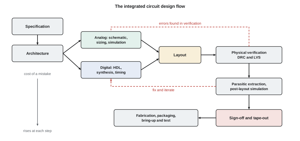
The specification states what the chip must do in measurable terms: functions, accuracy, speed, power, supply range, temperature range, package and cost. For CX-1 it runs to twenty pages, and Daniel insists that every number in it be traceable to a product requirement. The architecture divides the chip into blocks and allocates the specification among them: how much of the total error budget the reference may use, how much noise the preamplifier may add, how the counters share the 20 MHz clock. A good architecture makes each block's requirements clear enough that one designer can own it.
Analog blocks are then designed at the transistor level. The designer draws a schematic, chooses each device's width, length and bias current, and simulates the circuit with a SPICE-class simulator using the foundry's device models. Simulation is repeated across process corners, supply voltages and temperatures, and with Monte Carlo variation of the device parameters, until the block meets its requirements with margin. Digital blocks usually take a different path: the designer describes the logic in a hardware description language, as CMP-450 did for FPGAs, and a synthesis tool maps it onto a library of standard cells, small pre-designed and pre-characterized gates and flip-flops supplied with the process. A place-and-route tool then arranges the cells and wires them together, and static timing analysis checks every path against the clock.
Layout is the step that turns a schematic into the geometric shapes, layer by layer, that will become the photomasks. Analog layout is drawn largely by hand, because the placement of each device affects matching and noise; digital layout is generated by the tools. Physical verification then checks the layout in two ways. Design rule checking (DRC) confirms that every shape obeys the foundry's geometric rules: minimum widths, spacings, overlaps and densities. Layout versus schematic (LVS) extracts the circuit from the shapes and confirms that it is the same circuit as the schematic, with the same devices, sizes and connections. A layout can pass DRC and still be wrong, and LVS is the step that catches a missing contact or a transistor drawn at the wrong width.
Parasitic extraction then computes the resistance and capacitance of every wire and adds them to the netlist, and the critical blocks are simulated again with those parasitics. This post-layout simulation often shows that a circuit that was comfortable in schematic simulation is marginal once the wiring capacitance is included, and the designer returns to the schematic or the layout. When every block and the full chip pass their checks, the design team signs off and sends the final layout database to the foundry. The step is still called tape-out, from the days when the database left on magnetic tape.
Fabrication takes eight to twelve weeks for a mature process. The wafers come back, are diced into individual chips and packaged, and the team begins bring-up: powering the first parts on a test board, confirming that the serial interface responds, then measuring each block against the specification. For a product chip, characterization over temperature and supply on a sample of parts, qualification tests for reliability, and a production test program that checks every part follow. Lesson 12 returns to the whole flow at its end, when the CX-1 team runs its design review and tape-out checklist.
Who makes chips, and how small teams get access
Most chip companies today are fabless: they design chips and sell them, but they do not own a fabrication plant. Their designs are manufactured by foundries, companies whose business is running wafers for others. A foundry provides each customer with a process design kit (PDK) for each process it offers: the device models for simulation, the design rules, the rule decks for DRC and LVS, extraction rules, standard cell libraries and basic devices such as resistors, capacitors and protection structures. The PDK is the contract between designer and manufacturer. If a design follows the rules and the models are accurate, the foundry commits to building it as drawn.
A full mask set for a 180 nm process costs a few hundred thousand dollars, which would put custom silicon out of reach for a first prototype. Multi-project wafer (MPW) services solve this problem by combining many designs on one mask set and one wafer run and dividing the cost among them. A team buys a few square millimeters of a shared reticle and receives a few dozen packaged or bare prototypes.
In the US, MPW access for universities and small companies has long been provided by brokers that combine designs on shared runs; MOSIS, founded in 1981 and now relaunched as MOSIS 2.0 at the University of Southern California's Information Sciences Institute, is the best known. Cedarline's first CX-1 prototypes will be fabricated on a commercial MPW run, and the production version on a dedicated mask set at the same foundry. Open-source PDKs, in which a foundry publishes its design kit for anyone to use, have also changed the picture since about 2020; the 130 nm open PDK from SkyWater Technology is the best known. Shared shuttle services built on open PDKs have come and gone, and in 2025 the company that ran the best-known one closed, but community projects that let students and hobbyists put small designs on silicon have continued with other fabrication partners.
The economics of a custom chip
Daniel's question was partly about cost, and the answer depends on volume. A custom chip has a large fixed cost, the non-recurring engineering (NRE) of design, masks, prototypes, test development and qualification, and a small cost per unit. A board built from catalog parts has almost no NRE but a higher cost per unit. The chip route wins only when enough units are sold to spread its fixed cost.
The cost of a die starts with the wafer. A processed 200 mm wafer in a mature node costs on the order of one to two thousand dollars, depending on the number of mask layers and options. The number of dies on it follows from geometry, and the number of good dies from yield, the fraction of dies free of fatal defects. Random defects such as particles land on the wafer with some density D₀ per unit area; a die of area A survives if no defect lands on a critical part of it. The simplest model, Poisson statistics, gives a yield of e^{−AD₀}. Murphy's model, which allows the defect density to vary across wafers, gives a slightly more optimistic result for large dies. For small dies like CX-1 they agree.
Amara builds the comparison in a short script. The die is 2.4 mm on a side including its seal ring and the scribe line between dies. The board parts that CX-1 would replace cost about 4.80 dollars per product at Cedarline's volumes, and the team's estimate of total NRE, including its own engineering time, is 710 000 dollars.
import math

# Cost in dollars of the CX-1 mixed-signal chip versus the board it replaces (illustrative numbers)
wafer_d = 200.0          # wafer diameter, mm
wafer_cost = 1800.0      # processed 180 nm wafer, dollars
die_w, die_h = 2.4, 2.4  # die size including seal ring and scribe, mm
d0 = 0.25                # defect density, defects per cm^2

area = die_w * die_h
# gross dies per wafer: area term minus the edge loss term
gross = math.pi * (wafer_d / 2) ** 2 / area - math.pi * wafer_d / math.sqrt(2 * area)
gross = int(gross)
a_cm2 = area / 100.0
y_poisson = math.exp(-a_cm2 * d0)
y_murphy = ((1 - math.exp(-a_cm2 * d0)) / (a_cm2 * d0)) ** 2
good = int(gross * y_murphy)
die_cost = wafer_cost / good
pkg_test = 0.55          # package, final test and handling per part
chip = die_cost + pkg_test
print(f"die area {area:.2f} mm2, gross dies {gross}")
print(f"yield Poisson {y_poisson:.3f}, Murphy {y_murphy:.3f}, good dies {good}")
print(f"die cost {die_cost:.3f} dollars, packaged and tested {chip:.2f}")

board = 4.80             # parts the chip replaces on the current board
nre_mpw = 60000.0        # shuttle prototypes, tools time, test boards
nre_masks = 250000.0     # full mask set and production qualification
eng = 400000.0           # design team cost for the project
nre = nre_mpw + nre_masks + eng
saving = board - chip
print(f"saving per unit {saving:.2f} dollars, total NRE {nre:,.0f} dollars")
print(f"break-even volume {nre / saving:,.0f} units")
for vol in (10000, 50000, 100000, 250000):
print(f" {vol:>7,} units: chip route {chip + nre / vol:6.2f} per unit vs board {board:.2f}")die area 5.76 mm2, gross dies 5269 yield Poisson 0.986, Murphy 0.986, good dies 5193 die cost 0.347 dollars, packaged and tested 0.90 saving per unit 3.90 dollars, total NRE 710,000 dollars break-even volume 181,894 units 10,000 units: chip route 71.90 per unit vs board 4.80 50,000 units: chip route 15.10 per unit vs board 4.80 100,000 units: chip route 8.00 per unit vs board 4.80 250,000 units: chip route 3.74 per unit vs board 4.80
The die itself is almost free: about 5 200 good dies per wafer, 35 cents each. Packaging and test, not silicon, dominate the unit cost of a small chip in a mature node. The trouble is the NRE. At 10 000 units the chip route costs almost fifteen times as much per unit as the board; the two break even only at about 180 000 units. Cedarline ships roughly 40 000 detector channels and pedestrian stations a year, so over a five-year product life the chip only just pays for itself on parts cost alone.
Daniel's conclusion is that parts cost alone does not justify the project, but parts cost is not the whole argument. A chip that Cedarline owns cannot be discontinued by a supplier, which removes the cost of redesigns like last summer's. It draws a few milliwatts instead of the board's few hundred, which matters for the solar-powered pedestrian stations that Cedarline wants to sell for rural crossings. It shrinks the detector card to a quarter of its size. And the analog front end, designed once and well, will behave the same in every unit. With those benefits counted, management approves the project, on condition that the first prototypes come from a low-cost shared run before any money is spent on production masks.
Worked problem
Yield of a larger die
Suppose scope creep doubles the CX-1 die to 4.8 mm × 2.4 mm. With the same defect density of 0.25 per cm², what is the Poisson yield, and roughly how many good dies does a 200 mm wafer give?
Show solution
- The area is 11.52 mm² = 0.1152 cm², so AD₀ = 0.0288.
- \[Y = e^{-0.0288} = 0.972\]
- Gross dies: π(100)²/11.52 − π(200)/√(23.04) = 2727 − 131 ≈ 2600.
- Good dies ≈ 2600 × 0.972 ≈ 2530.
Answer: About 97 % yield and roughly 2 500 good dies: doubling the area halves the dies per wafer and costs a little more yield. For small dies, area rather than yield drives cost.
Analog and digital design styles
The two halves of CX-1 are designed in very different ways, and a mixed-signal designer must be comfortable with both. Digital design is about abstraction. A designer writes logic, a synthesis tool builds it from standard cells whose delays and power have already been characterized, and timing analysis proves that every path meets the clock. The individual transistor almost disappears. Lessons 4 to 6 open up the cells to show what is inside them, because understanding why a gate has the delay it has is what makes a digital designer effective, and because full-custom digital circuits are still drawn by hand where speed or area matter.
Analog design is about the transistor. The preamplifier's gain, noise and offset depend directly on the width, length and bias current of each device and on how well pairs of devices match. There is no synthesis tool that turns an op-amp specification into a working layout, though tools that help size circuits are improving. The analog designer works from hand analysis, using simple models to choose a starting design, then refines it in simulation. Lessons 3 and 8 to 11 develop the hand-analysis methods that make this possible, centered on the gm/ID approach that has become the standard way to size transistors in modern processes.
Mixing the two on one die brings problems that neither half has alone. Digital circuits switch fast and inject current spikes into the shared substrate and supply wires; analog circuits are sensitive to microvolts. Lesson 7 covers the layout techniques, such as separate supplies, guard rings and careful placement, that keep the counter's 20 MHz clock out of the microphone preamplifier.
Planning the CX-1 project
Priya draws up a plan that follows the flow. The first two months go to architecture and the critical analog blocks: the reference, the bias generator, the preamplifier and the data converter, which carry most of the technical risk. The digital counters and serial interface, which are straightforward, are written in parallel. Layout follows block by block, and the full chip is assembled, verified and simulated in month five. The first tape-out is to a shared run, with a die that includes test structures, such as isolated transistors, resistor and capacitor arrays and a ring oscillator, so that Leo can measure the process itself as well as the circuits.
Daniel adds one rule that Priya's former employer also followed: no block goes to layout until its schematic has passed a design review in which someone other than the designer has checked the hand analysis, the simulation results across corners, and the test plan for that block. Every review and every simulation result goes into a design record that lesson 12 will use as the basis for the tape-out decision.
Common mistakes
MistakeThinking that a custom chip is always cheaper than catalog parts.
InsteadBelow the break-even volume the NRE dominates; the case for a chip often rests on power, size, supply security or performance.
MistakeTreating a layout that passes DRC as correct.
InsteadDRC checks geometry only; LVS confirms that the layout is the intended circuit, and post-layout simulation confirms that it still works.
MistakeAssuming the die is the main unit cost of a small chip.
InsteadFor small dies in mature nodes, packaging and test usually cost more than the silicon.
MistakeDesigning analog blocks from schematic simulation alone.
InsteadWiring parasitics and device mismatch can make a block fail after layout; post-layout and Monte Carlo simulation are part of the design.
Summary and key terms
- An integrated circuit is designed through specification, architecture, circuit or logic design, layout, physical verification, parasitic extraction, sign-off and tape-out, then fabricated, packaged and tested.
- Analog blocks are designed at the transistor level with hand analysis and simulation; digital blocks are synthesized from standard cells and checked by static timing analysis.
- DRC checks the layout geometry, and LVS checks that the layout is the same circuit as the schematic.
- Fabless companies design chips that foundries manufacture using a process design kit; multi-project wafer runs share mask costs among many designs.
- Good dies per wafer follow from die area and defect density; for small dies in mature nodes the die is cheap and NRE dominates.
- CX-1 is a 180 nm mixed-signal chip combining the loop detector front end and counters with the APS-2 audio front end and data converter.
- Process design kit (PDK)
- The foundry-supplied models, rules, decks and libraries needed to design for a process.
- Design rule check (DRC)
- Verification that a layout obeys the foundry's geometric rules.
- Layout versus schematic (LVS)
- Verification that the circuit extracted from a layout matches the schematic.
- Parasitic extraction
- Computing the resistance and capacitance of the layout's wires for post-layout simulation.
- Tape-out
- Release of the final layout database to the foundry for mask making.
- Multi-project wafer (MPW)
- A fabrication run that shares one mask set among many designs.
- Non-recurring engineering (NRE)
- The fixed cost of developing a product, paid once regardless of volume.
- Yield
- The fraction of manufactured dies that work.
Practice problems
Work each problem on paper first, then reveal the answer to check.
A wafer costs 1 800 dollars and yields 5 193 good dies. What is the die cost?
Show answer
1 800/5 193 ≈ 0.35 dollars.
Find the Poisson yield of a 10 mm² die at D₀ = 0.5 per cm².
Show answer
AD₀ = 0.1 × 0.5 = 0.05; Y = e^{−0.05} ≈ 0.951.
NRE is 500 000 dollars and the chip saves 2.50 dollars per unit. What is the break-even volume?
Show answer
200 000 units.
A layout passes DRC but the chip does not work. Name a check that might have caught the problem.
Show answer
LVS, which compares the extracted circuit with the schematic; or post-layout simulation.
Why is the CX-1 microcontroller kept off the chip?
Show answer
It is cheap as a catalog part, its software changes often, and integrating it would add risk to a first chip.
Give two benefits of CX-1 other than parts cost.
Show answer
No supplier discontinuations, much lower power, smaller boards, consistent analog performance.
Lesson quiz · 5 questions
Score 60% or more to complete this lesson.
Create a free account to save your progress, take quizzes and earn a certificate.