
ELE-445 · Lesson 2 of 12 · 25 min
CMOS fabrication and process technology
Before Priya lets anyone draw a transistor, she spends a morning with the team on the process itself. A designer who knows only the schematic symbols treats the chip as an abstract circuit; a designer who knows how the layers are made understands why the design rules exist, which devices match well, where parasitic diodes and transistors hide, and why a resistor drawn in one layer varies by twenty percent while a capacitor drawn in another varies by ten. This lesson follows a wafer through a simplified CMOS process, introduces the layers that the CX-1 layout will use, and designs the first passive devices on the chip.
From silicon wafer to transistor
A CMOS process starts with a lightly doped p-type silicon wafer, polished flat, about 0.7 mm thick and 200 mm in diameter for a 180 nm process. Every structure on the chip is built in or on its top few micrometers; the rest of the wafer is mechanical support. The process is a long sequence of steps, often several hundred, but they repeat a small number of operations. Photolithography transfers a pattern from a mask to a light-sensitive resist on the wafer. Etching removes material where the resist is open. Ion implantation fires dopant atoms into the silicon where the resist is open, and annealing repairs the damage and activates the dopants. Deposition adds layers of oxide, polysilicon or metal, and chemical-mechanical polishing (CMP) planarizes the surface so the next layer can be patterned accurately.
Each mask defines one layer, and the order of the layers follows the order of fabrication. A simplified 180 nm CMOS sequence runs as follows.
| Step | What it makes | Why it matters to the designer |
|---|---|---|
| Shallow trench isolation (STI) | Oxide-filled trenches between active areas | Defines where transistors can be; stress from the trench edge shifts nearby devices |
| N-well and p-well implants | Regions for PMOS and NMOS devices | Wells are large, and their spacing rules set the density of mixed layouts |
| Threshold adjust implants | Doping under the gate | Sets VT; separate implants give core and I/O devices |
| Gate oxide growth | About 4 nm of oxide for core devices | Sets Cox and the maximum gate voltage |
| Polysilicon deposition and etch | Transistor gates and poly wires and resistors | The gate length is the poly width over active area |
| Source and drain implants | n+ and p+ regions, self-aligned to the gate | Self-alignment makes the channel length set by the poly line |
| Silicide | Low-resistance metal-silicon compound on gates and diffusions | Blocked where high-value resistors are needed |
| Contacts and metal layers | Tungsten contacts, then five or six aluminum or copper layers with vias | Wiring resistance, capacitance and current density limits |
| Passivation | Protective nitride and oxide with openings over pads | Pads must be opened to bond wires |
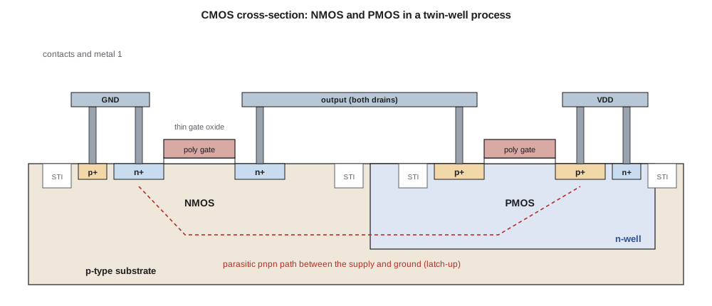
The cross-section shows the two transistor types side by side. The NMOS transistor sits in the p-type substrate or a p-well; its source and drain are heavily doped n+ regions, and its channel forms at the silicon surface under the gate when the gate is driven positive. The PMOS transistor sits in an n-well; its source and drain are p+ regions. Because the well and the substrate form a pn junction, the n-well must always be biased at or above the substrate so that the junction stays reverse-biased. In a standard process the substrate is tied to ground and every n-well to the positive supply or to the source of its PMOS devices.
The self-aligned gate is the trick that made CMOS scale. The polysilicon gate is patterned first, and the source and drain implants that follow use the gate itself as a mask. The channel length is therefore set by the width of the poly line, which lithography controls tightly, rather than by the alignment between two masks. The nominal 180 nm of the process name is the minimum drawn gate length; the effective electrical channel is somewhat shorter because the source and drain diffuse slightly under the gate edges.
Layers, design rules and lambda
Design rules translate the limits of the process into geometry. Every layer has a minimum width and a minimum spacing; layers that must overlap have minimum enclosures, such as how far active area must extend past a contact or how far poly must extend past active area to make sure the gate cuts all the way across the channel. There are also density rules, which require each layer to cover a minimum and maximum fraction of every region of the chip so that chemical-mechanical polishing leaves a flat surface, and antenna rules, which limit how much metal can be connected to a gate during fabrication, before the diffusion that will protect it is wired in. A long metal line attached only to a gate collects charge from the plasma etch and can damage the thin oxide, so the layout either breaks the line with a jumper to a higher metal or adds a small protection diode.
Older textbooks express rules in units of λ, half the minimum feature size, so that a design could be scaled from one process generation to the next by changing λ alone. Modern rule sets are written in absolute dimensions and contain far too many special cases for λ scaling to work, but λ rules remain a good way to learn. In λ units a minimum transistor needs a gate 2λ long, active area extending 3λ past the gate on each side for contacts and a contact 2λ square, which makes a minimum transistor about 8λ by 6λ. In the illustrative CX-1 process λ is 90 nm.
Two kinds of transistor
The process offers core transistors with a 4 nm gate oxide, rated for 1.8 V, and input/output transistors with a thicker oxide of about 7 nm, rated for 3.3 V. Core transistors are faster and denser; I/O transistors are slower but tolerate the higher voltage, and they are used at the pads, in level shifters and, often, in analog circuits that need more signal swing than 1.8 V allows. The CX-1 loop oscillator drivers run from 3.3 V to put more signal into the loop, while the counters and the serial interface run at 1.8 V to save power. The oxide capacitance per unit area, Cox, follows from the oxide thickness and sets both the transistor's current-carrying ability and the capacitance it presents to the circuit that drives its gate.
Resistors on a chip
Integrated resistors are drawn as strips of a resistive layer, and their value is set by the layer's sheet resistance R_s, the resistance of one square of the layer, multiplied by the number of squares: R = R_s L/W. Because resistance depends only on the ratio L/W for a given layer, a 1 µm by 1 µm square and a 10 µm by 10 µm square have the same resistance. The contact heads at each end add a fixed amount, and the effective width is slightly less than the drawn width because the edges etch back, which is one reason precise resistors are drawn wider than the minimum.
| Layer | Sheet resistance | Typical use | Typical spread |
|---|---|---|---|
| Silicided poly or diffusion | 5–10 Ω/□ | Wiring and gates; not a resistor layer | Large |
| Unsilicided n+ or p+ poly | 100–300 Ω/□ | Moderate resistors | ±15–20 % |
| High-resistance poly | About 1 kΩ/□ | Bias resistors, large values | ±20 % |
| N-well | 1–2 kΩ/□ | Large, voltage-dependent resistors | ±30 %, strong voltage coefficient |
| Metal 1 | About 0.08 Ω/□ | Wiring | Small |
The CX-1 bias generator needs a 400 kΩ resistor. Drawn in silicided poly it would be absurdly long, so Priya chooses the process's high-resistance poly option, in which a silicide-block mask keeps the silicide off the resistor body. She also notes the resistor's spread and temperature coefficient, because they will set how much the bias currents vary.
# Passive devices on the course's illustrative 180 nm process
eps_ox = 3.9 * 8.854e-12      # F/m
tox = 4.0e-9                  # gate oxide thickness, m
cox = eps_ox / tox            # F/m^2
print(f"gate oxide Cox = {cox * 1e3:.2f} fF/um^2")

# A 400 kilohm bias resistor in high-resistance poly
rs_hipo = 1000.0              # ohms per square
w = 1.0                       # drawn width, um
r_contact = 2 * 50.0          # two contact heads, ohms
target = 400e3
squares = (target - r_contact) / rs_hipo
length = squares * w
print(f"high-res poly: {squares:.1f} squares, length {length:.0f} um at W = {w} um")
# fold it into a serpentine of 40 um legs at a 2 um pitch
legs = int(length // 40) + 1
print(f"  folded into {legs} legs of 40 um: about {legs * 2.0:.0f} um x 40 um")
# the same resistor in silicided poly (8 ohms/sq) would be absurd
print(f"  in silicided poly it would need {target / 8.0 / 1000:.0f} mm of track")

# Process spread and temperature on that resistor
for corner, f in (("high (+20 %)", 1.2), ("typical", 1.0), ("low (-20 %)", 0.8)):
    print(f"  {corner:<13} R = {target * f / 1e3:.0f} kohm")
tc = -1.0e-3                  # per kelvin, high-res poly is typically negative
for t in (-40, 27, 125):
    print(f"  at {t:>4} C: {target * (1 + tc * (t - 27)) / 1e3:.0f} kohm")

# A 2 pF MIM capacitor and a 2 pF gate-oxide (MOS) capacitor
c_mim = 2.0e-3                # F/m^2 (2 fF/um^2)
side_mim = (2e-12 / c_mim) ** 0.5 * 1e6
side_mos = (2e-12 / cox) ** 0.5 * 1e6
print(f"2 pF MIM: {side_mim:.1f} um square; 2 pF MOS: {side_mos:.1f} um square")gate oxide Cox = 8.63 fF/um^2 high-res poly: 399.9 squares, length 400 um at W = 1.0 um folded into 10 legs of 40 um: about 20 um x 40 um in silicided poly it would need 50 mm of track high (+20 %) R = 480 kohm typical R = 400 kohm low (-20 %) R = 320 kohm at -40 C: 427 kohm at 27 C: 400 kohm at 125 C: 361 kohm 2 pF MIM: 31.6 um square; 2 pF MOS: 15.2 um square
Four hundred squares at 1 µm wide makes a 400 µm strip, which Priya folds into ten legs of 40 µm to give a block about 20 µm by 40 µm. The absolute value will vary by about ±20 % from wafer to wafer, and by about ten percent over the temperature range because high-resistance poly has a negative temperature coefficient. Neither is acceptable for an absolute specification, which is why the CX-1 design never relies on the absolute value of a resistor where it can rely on a ratio. Two resistors drawn from the same layer, side by side, with the same width and orientation, match to a fraction of a percent even when their absolute values are twenty percent off. Lessons 7 and 8 use that property again and again.
Worked problem
Ratio accuracy versus absolute accuracy
A gain stage uses a 10 kΩ input resistor and a 250 kΩ feedback resistor in unsilicided poly, giving a gain of 25. The process spread is ±20 % and the two resistors are drawn as matched units. Estimate the variation in the gain and in each resistor value.
Show solution
- Each resistor can be 20 % high or low from wafer to wafer, so each absolute value ranges over roughly 8–12 kΩ and 200–300 kΩ.
- Both resistors move together because they are made in the same layer at the same time, so the ratio is set by their matching, typically 0.1–0.5 % for well-drawn units.
- \[A = \frac{R_f}{R_i} = \frac{25 R_u}{R_u} = 25 \pm \approx 0.3\ \%\]
Answer: The gain varies by a few tenths of a percent while each resistor varies by twenty percent. Integrated circuits are designed around ratios.
Capacitors on a chip
Capacitors matter in almost every analog block on CX-1: the op-amp's compensation capacitor, the sampling capacitors of the data converter and the filter capacitors of the reference. A 180 nm process offers several kinds. The MOS capacitor uses a transistor's gate oxide and has the highest capacitance per area, about 8.6 fF/µm², but its value depends strongly on the voltage across it, because the channel under the gate forms or disappears with the bias. The metal-insulator-metal (MIM) capacitor is an optional module that adds a thin dielectric between two special metal plates near the top of the stack, at about 1–2 fF/µm², with very low voltage coefficient and good matching. Metal-oxide-metal (MOM) capacitors use the lateral fringing between interdigitated fingers of ordinary metal layers and need no extra masks; they are widely used in data converters on processes without a MIM module.
The script compares a 2 pF MIM capacitor, 32 µm on a side, with a 2 pF MOS capacitor of 15 µm on a side. Priya chooses MIM for the data converter, where linearity and matching matter, and uses MOS capacitors only for supply decoupling, where nonlinearity does not matter and density does.
Parasitic devices and latch-up
The layers of a CMOS process form devices that nobody drew. Every source and drain is a diode to its well or substrate. Every wire is a capacitor to the substrate and to its neighbors. Most important, the n+ source of an NMOS transistor, the p substrate and the n-well form a lateral NPN transistor, and the p+ source of a PMOS transistor, the n-well and the substrate form a vertical PNP transistor. Together they make a four-layer pnpn structure, a thyristor, connected directly between the supply and ground.
Normally both parasitic transistors are off, because the well and substrate are tied to their supplies. But if a current pulse, from a voltage spike on a pin, a fast supply transient or radiation, raises the local substrate potential near an NMOS source or lowers the local well potential near a PMOS source, one parasitic transistor can turn on, its collector current turns on the other, and the pair latches into a low-resistance path from supply to ground. The chip draws a large current until the power is removed and may be destroyed. This is latch-up, and preventing it is a layout discipline. Substrate and well contacts are placed frequently, every few tens of micrometers, so that the resistances that would let the local potential rise are small; guard rings of contacts surround circuits connected to pins; and the spacing between NMOS and PMOS devices near the pads is increased. The foundry's design rules include latch-up rules, and lesson 12 adds the latch-up and electrostatic discharge checks to the tape-out list.
Variation: where the numbers come from
No two transistors on a wafer are identical, and the designer needs to know how they differ. Variation comes in two kinds. Global, or inter-die, variation shifts every device on a die together: the gate oxide is slightly thicker on one wafer, or a threshold implant slightly heavier. Foundries capture it with process corners, model sets that represent the slow and fast extremes of NMOS and PMOS behavior; the names TT, SS, FF, SF and FS give the NMOS speed first and the PMOS speed second. Local, or intra-die, variation makes neighboring devices differ: random fluctuations in the number and position of dopant atoms under each gate, roughness at the gate edges, and gradients across the die. Local variation is captured by mismatch models, usually expressed by Pelgrom's law, which says that the standard deviation of the difference between two identical devices falls as one over the square root of their area. Lesson 7 develops that law and the layout techniques that exploit it.
The distinction drives the whole design philosophy of analog integrated circuits. Global variation is large but common to all devices, so designs that depend on ratios and matching tolerate it. Local variation is small but random, so designs that need precise matching use large devices and careful layout. The CX-1 resistor's ±20 % is global; its 0.3 % match to its neighbor is local.
Common mistakes
MistakeSpecifying an absolute resistor value as if it were accurate.
InsteadIntegrated resistors vary by ±15–30 % from wafer to wafer; design with ratios or trim the value.
MistakeUsing a MOS capacitor in a signal path that needs linearity.
InsteadMOS capacitance changes with the voltage across it; use MIM or MOM capacitors for signals.
MistakeLeaving long metal lines connected only to a gate.
InsteadAntenna rules exist because plasma charge collected on the metal can damage the gate oxide during fabrication.
MistakeSkimping on substrate and well contacts to save area.
InsteadSparse ties raise the substrate resistance that triggers latch-up.
Summary and key terms
- CMOS is built from a p-type wafer by repeated lithography, etching, implantation, deposition and polishing; each mask defines one layer.
- NMOS transistors sit in the p substrate or p-well and PMOS transistors in n-wells; the self-aligned gate makes the channel length equal to the poly width.
- Design rules set minimum widths, spacings, enclosures, densities and antenna limits; λ rules are a useful teaching approximation.
- Integrated resistors are R_s L/W plus contact resistance; their absolute values vary widely but matched resistors track closely.
- MOS capacitors are dense but nonlinear; MIM and MOM capacitors are linear and match well.
- The parasitic pnpn structure in CMOS can latch up; frequent substrate and well ties and guard rings prevent it.
- Global variation is captured by process corners and local variation by mismatch models.
- Shallow trench isolation
- Oxide-filled trenches that separate active areas.
- Self-aligned gate
- A process in which the gate itself masks the source and drain implants.
- Sheet resistance
- The resistance of one square of a layer, in ohms per square.
- MIM capacitor
- A metal-insulator-metal capacitor formed by an optional thin dielectric between special metal plates.
- Latch-up
- Triggering of the parasitic pnpn thyristor in CMOS, causing a destructive supply-to-ground current.
- Antenna rule
- A limit on the metal area connected to a gate during fabrication.
- Process corner
- A model set representing a slow or fast extreme of global process variation.
- Mismatch
- Random differences between nominally identical, nearby devices.
Practice problems
Work each problem on paper first, then reveal the answer to check.
A 50 kΩ resistor is drawn in 200 Ω/□ poly at 2 µm wide. Ignoring contacts, how long is it?
Show answer
250 squares, so 500 µm.
What area does a 1 pF MIM capacitor need at 2 fF/µm²?
Show answer
500 µm², about 22 µm square.
Why must every n-well be biased at or above the substrate?
Show answer
To keep the well-substrate junction reverse-biased.
Which process corner has slow NMOS and fast PMOS?
Show answer
SF.
Two matched resistors each vary by ±20 % absolute. How much does their ratio vary?
Show answer
Only by their mismatch, typically a few tenths of a percent.
Name two layout measures that prevent latch-up.
Show answer
Frequent substrate and well contacts; guard rings; extra spacing between NMOS and PMOS near pads.
Lesson quiz · 5 questions
Score 60% or more to complete this lesson.
Create a free account to save your progress, take quizzes and earn a certificate.