
ELE-315 · Lesson 2 of 12 · 20 min
Microcontroller architecture: core, memory map, buses and clocks
Before Jonah can change a single line of the NS-4 firmware, he needs a mental model of the chip it runs on. A microcontroller looks like one black square on the board, but inside it is a small city: a processor core, memories, a set of buses that carry traffic between them, dozens of peripherals, and a clock system that sets the pace for all of it. Firmware controls this city almost entirely by reading and writing particular addresses. This lesson builds the model: what the core does, how the memory map gives every resource an address, how buses and bridges connect masters to slaves, and how the clock tree and reset logic bring the chip to life.
The NS-4 uses a 32-bit microcontroller with a three-stage pipelined RISC core, 256 KB of flash and 64 KB of SRAM, running at 48 MHz. The NS-5 prototype uses a microcontroller built around a RISC-V core of the kind chosen in CMP-310, with 512 KB of flash, 128 KB of SRAM and a small integer accelerator. The two chips come from different vendors and their reference manuals look nothing alike, yet the same architectural ideas appear in both, which is the point of learning the ideas rather than one vendor's register names.
The processor core
Microcontroller cores are deliberately simple. Most are 32-bit RISC designs with a short pipeline of two to five stages, a single issue slot, no data cache and often a small instruction cache or a flash prefetch buffer. They implement a load-store instruction set, have 16 or 32 general-purpose registers, and support a compact 16-bit instruction encoding to save flash. Many include a hardware multiplier, some a hardware divider, and the larger ones a single-precision floating-point unit and digital signal processing instructions such as multiply-accumulate and saturating arithmetic. These choices favor small silicon area, low power and predictable timing over raw speed, because a microcontroller usually spends most of its time asleep and must respond to events with a known worst-case delay.
Two features distinguish microcontroller cores from the processors of CMP-310. The first is the interrupt controller, tightly coupled to the core, which can save registers and jump to a handler within a dozen cycles of an event; lesson 7 covers it. The second is a set of low-power states in which the clock to the core stops while peripherals keep working; lesson 11 covers those. Many cores also include a system timer for periodic ticks, a memory protection unit that can stop errant code from writing where it should not, and a debug unit that lets a probe halt the core, read registers and set breakpoints through two pins.
The memory map
A microcontroller has one address space, typically 32 bits wide, and every resource the core can reach has an address in it. Flash, SRAM, peripheral registers, the interrupt controller and the debug unit all occupy fixed regions. Reading address 0x0800 1000 fetches a word of program flash; reading address 0x4001 0800 reads a status register of a serial port. This is memory-mapped I/O: there are no special input-output instructions, only loads and stores to addresses that happen to be wired to hardware rather than memory. The memory map, a table in the reference manual, is therefore the first page a firmware engineer bookmarks.
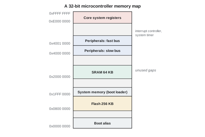
Several features of the map are worth noticing. The regions are sparse: 256 KB of flash and 64 KB of SRAM fill a tiny fraction of a 4 GB space, and accesses to unused addresses cause a bus fault. Address 0 often aliases another region, typically flash, so that the core can find its reset vector at a fixed place. Peripheral registers are grouped by bus, because the bus determines the access speed and the clock that must be enabled before the registers respond. And a few regions have special behavior: bit-band aliases on some cores let a single store set or clear one bit, and the core's private system region holds registers that only privileged code may touch.
| Region | NS-4 base address | Size | Contents |
|---|---|---|---|
| Flash | 0x0800 0000 | 256 KB | Program code, constants, vector table |
| System memory | 0x1FFF 0000 | 28 KB | Factory boot loader |
| SRAM | 0x2000 0000 | 64 KB | Variables, stack, heap if any, buffers |
| Peripheral bus 1 | 0x4000 0000 | 64 KB | Slow peripherals: UARTs, I2C, timers 2 to 5, watchdog |
| Peripheral bus 2 | 0x4001 0000 | 64 KB | Fast peripherals: SPI, ADC, timer 1, GPIO ports |
| Core system | 0xE000 0000 | 1 MB | Interrupt controller, system timer, debug, MPU |
Buses, masters and slaves
Inside the chip, a bus matrix connects masters, which start transfers, to slaves, which respond. The core is a master, usually with separate instruction and data ports so it can fetch and load at once; a direct memory access controller is another master; on bigger chips a USB or Ethernet controller may be a third. Flash, SRAM and peripheral buses are slaves. A crossbar-style matrix lets different masters reach different slaves at the same time, so the DMA controller can copy ADC results into one SRAM bank while the core runs code from flash. When two masters want the same slave, an arbiter decides who waits.
Peripherals do not sit on the fast matrix directly. They hang off slower peripheral buses reached through bridges, which translate between the high-speed protocol of the matrix and a simpler protocol suited to registers. Each peripheral bus has its own clock, often divided down from the core clock to save power, and an access to a peripheral register can take several core cycles. This explains a surprise Jonah meets on the bench: a loop that toggles a pin by writing a GPIO register runs slower than the instruction count suggests, because each store crosses a bridge.
Flash, SRAM and wait states
Program flash on a microcontroller is slow compared with the core. A typical embedded flash array has an access time of 20 to 40 ns, while a 48 MHz core cycle is about 21 ns and a 200 MHz cycle is 5 ns. To keep the core fed, the flash controller inserts wait states, extra cycles per access, and compensates with a wide interface that reads 64 or 128 bits at once plus a prefetch buffer or small cache that streams sequential instructions. Branch-heavy code still stalls on flash. SRAM, by contrast, is single-cycle at the core clock, so time-critical routines such as interrupt handlers are sometimes copied into SRAM at start-up and run from there.
Worked problem
Choosing flash wait states
The NS-4 flash has a worst-case access time of 35 ns across the full temperature range. How many wait states must the firmware configure at 24 MHz, at 48 MHz and at 72 MHz?
Show solution
- \[ T_{24} = 41.7\ \text{ns} \Rightarrow \lceil 35/41.7 \rceil - 1 = 0\]
- \[ T_{48} = 20.8\ \text{ns} \Rightarrow \lceil 35/20.8 \rceil - 1 = 1\]
- \[ T_{72} = 13.9\ \text{ns} \Rightarrow \lceil 35/13.9 \rceil - 1 = 2\]
Answer: No wait states at 24 MHz, one at 48 MHz and two at 72 MHz. The wait-state setting must be raised before the clock is raised, or the core will read garbage from flash.
That ordering rule is a classic start-up bug. If firmware switches the system clock to 72 MHz while the flash controller is still set for zero wait states, the very next instruction fetch may return corrupted data and the core crashes in ways that are hard to diagnose. The correct sequence is: set the wait states for the target frequency, confirm the setting took effect, then switch the clock; when lowering the clock, switch first and reduce wait states afterwards.
The clock tree
Every synchronous block on the chip needs a clock, and the clock tree is the network that generates, selects, divides and gates those clocks. Sources include an internal RC oscillator, fast to start but accurate only to about one percent; an external crystal oscillator, accurate to tens of parts per million; a low-frequency 32.768 kHz crystal for the real-time clock; and a phase-locked loop that multiplies a reference up to the core frequency. Multiplexers select the system clock source, prescalers divide it for each bus, and individual gates enable the clock to each peripheral. A peripheral whose clock gate is off does not respond to register writes at all, which is the single most common reason a newly written driver appears dead.
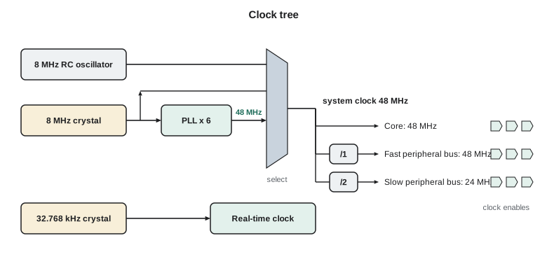
The NS-4 starts on its internal RC oscillator, because that runs as soon as power is applied. Start-up code then enables the 8 MHz crystal, waits for it to stabilize, configures the PLL to multiply by six, waits for the PLL to lock, raises the flash wait states, and finally switches the system clock to the 48 MHz PLL output. Peripheral bus 1 runs at 24 MHz and peripheral bus 2 at 48 MHz. The 32.768 kHz crystal, which is 2¹⁵ Hz so that a 15-bit counter overflows exactly once per second, runs the real-time clock even while the main clocks are stopped in deep sleep.
# Search PLL settings that give a target system clock from an 8 MHz crystal
f_in = 8.0      # MHz
target = 48.0   # MHz
results = []
for m in range(1, 9):              # input divider
    f_ref = f_in / m
    if not (1.0 <= f_ref <= 4.0):  # PLL reference must lie in this window
        continue
    for n in range(8, 101):        # feedback multiplier
        f_vco = f_ref * n
        if not (96.0 <= f_vco <= 344.0):
            continue
        for p in (2, 4, 6, 8):     # output divider
            f_out = f_vco / p
            if abs(f_out - target) < 1e-9:
                results.append((m, n, p, f_ref, f_vco))
print(len(results), "exact settings found; first five:")
for m, n, p, f_ref, f_vco in results[:5]:
print(f"M={m} N={n:3d} P={p} ref {f_ref:.2f} MHz VCO {f_vco:6.1f} MHz out {f_vco/p:.1f} MHz")11 exact settings found; first five: M=2 N= 24 P=2 ref 4.00 MHz VCO 96.0 MHz out 48.0 MHz M=2 N= 48 P=4 ref 4.00 MHz VCO 192.0 MHz out 48.0 MHz M=2 N= 72 P=6 ref 4.00 MHz VCO 288.0 MHz out 48.0 MHz M=3 N= 36 P=2 ref 2.67 MHz VCO 96.0 MHz out 48.0 MHz M=3 N= 72 P=4 ref 2.67 MHz VCO 192.0 MHz out 48.0 MHz
Several settings work. Engineers usually prefer the lowest voltage-controlled oscillator frequency that meets the constraints, because it draws less power, and a reference near the top of its window, because jitter falls as the reference rises. The vendor's configuration tool does this search too, but knowing how it works lets Jonah check the tool and explain why a clock comes out at 47.9 MHz instead of 48.
Reset and start-up
A microcontroller resets on power-up, when the supply falls below the brown-out threshold, when the reset pin is pulled low, when the watchdog expires, or when software requests it. After reset the core reads two words from the vector table at the start of flash: the initial stack pointer and the address of the reset handler. It then runs the reset handler, which on most projects is start-up code supplied with the toolchain. That code copies initialized variables from flash to SRAM, clears uninitialized variables to zero, sets up the clocks and calls main. Lesson 3 looks at this code in detail. A reset-cause register records why the last reset happened, and good firmware logs it: an NS-4 that reports a string of watchdog resets is telling the team something.
/* A minimal vector table in C, placed at the start of flash by the linker */
extern unsigned long _estack;          /* top of SRAM, defined in the linker script */
void Reset_Handler(void);
void Default_Handler(void) { for (;;) { } }
void SysTick_Handler(void)  __attribute__((weak, alias("Default_Handler")));
void USART2_IRQHandler(void) __attribute__((weak, alias("Default_Handler")));

__attribute__((section(".isr_vector")))
const void *vector_table[] = {
    &_estack,              /* 0: initial stack pointer      */
    Reset_Handler,         /* 1: reset                      */
    Default_Handler,       /* 2: non-maskable interrupt     */
    Default_Handler,       /* 3: hard fault                 */
    /* ... system exceptions ... */
    SysTick_Handler,       /* system timer tick             */
    /* ... peripheral interrupts in vendor order ... */
    USART2_IRQHandler,
};
Choosing a microcontroller
When Ines chose the NS-5's microcontroller, she weighed far more than the core. The checklist covered flash and SRAM with a margin for growth; the number and type of peripherals, including two SPI ports, two I²C ports, three UARTs and a CAN controller; ADC resolution and sample rate; sleep current with the real-time clock running; operating temperature grade; package size and pin count; supply voltage range; security features such as secure boot and a hardware cryptographic engine; the quality of the vendor's documentation, errata and tools; long-term availability, because a part that goes out of production forces a redesign; and price at the expected volume. CMP-310's trade study chose the core; this list chose the chip around it.
Common mistakes
MistakeWriting to a peripheral before enabling its clock.
InsteadEnable the peripheral's clock gate first; until then its registers ignore writes and read as zero.
MistakeRaising the core clock before raising the flash wait states.
InsteadSet wait states for the higher frequency first, then switch the clock; reverse the order when slowing down.
MistakeAssuming a peripheral register access takes one cycle.
InsteadPeripheral buses run through bridges at divided clocks; register accesses can take several core cycles.
MistakeTrusting the internal RC oscillator for serial timing.
InsteadRC oscillators drift by around a percent with temperature; use a crystal for UARTs and CAN at higher bit rates.
MistakeIgnoring the reset-cause register.
InsteadRead and log the reset cause at start-up; repeated watchdog or brown-out resets reveal field problems.
Summary and key terms
- Microcontroller cores are simple, low-power, predictable 32-bit RISC designs with fast interrupt entry.
- Every resource has an address in one memory map; peripherals are controlled by loads and stores.
- A bus matrix connects masters such as the core and DMA to slaves such as flash, SRAM and bridges.
- Flash needs wait states at higher clocks; SRAM is single-cycle.
- The clock tree selects, multiplies, divides and gates clocks; peripheral clocks must be enabled.
- After reset the core loads the stack pointer and reset vector, and start-up code prepares memory and clocks.
- Choosing an MCU weighs peripherals, memory, power, temperature, security, tools and availability.
- Memory-mapped I/O
- Controlling hardware by reading and writing addresses that map to device registers.
- Memory map
- The table of address regions assigned to flash, SRAM, peripherals and system registers.
- Bus matrix
- The on-chip interconnect that links masters to slaves and arbitrates conflicts.
- Wait state
- An extra clock cycle inserted while a slow memory completes an access.
- PLL
- Phase-locked loop: a circuit that multiplies a reference clock to a higher frequency.
- Clock gating
- Turning off the clock to a block to save power; a gated peripheral does not respond.
- Vector table
- The table at the start of memory holding the initial stack pointer and handler addresses.
- Brown-out reset
- A reset triggered when the supply voltage falls below a safe threshold.
Practice problems
Work each problem on paper first, then reveal the answer to check.
A flash array needs 28 ns per access. How many wait states are needed at 80 MHz?
Show answer
T = 12.5 ns; ⌈28/12.5⌉ − 1 = 3 − 1 = 2 wait states.
An 8 MHz crystal feeds a PLL with M = 2, N = 36, P = 2. What are the reference, oscillator and output frequencies?
Show answer
Reference 4 MHz, oscillator 144 MHz, output 72 MHz.
Why does a 32.768 kHz crystal suit a real-time clock?
Show answer
32,768 = 2¹⁵, so a 15-bit binary counter overflows exactly once per second.
A new UART driver writes its registers but nothing happens and the registers read back zero. What should you check first?
Show answer
Whether the UART's peripheral clock gate is enabled.
Lesson quiz · 5 questions
Score 60% or more to complete this lesson.
Create a free account to save your progress, take quizzes and earn a certificate.