
ELE-202 · Lesson 9 of 12 · 34 min
Op amp applications: sensing, comparators and data conversion
Lesson 8 analyzed the basic op amp circuits using the ideal model. This lesson applies them to the job op amps most often do: connecting the physical world to digital systems. A temperature, pressure, strain or current sensor produces a small voltage or current, often riding on a large common-mode voltage and surrounded by electrical noise. Op amp circuits amplify it accurately, convert it to a standard signal, compare it with a threshold, and present it to an analog-to-digital converter. Along the way we meet the limits of real op amps that matter most in DC measurement: offset, bias current and finite common-mode rejection.
Measuring differences: common-mode rejection
Many sensors produce a small difference between two voltages that both sit at a much larger common level. The strain gauge bridge of Lesson 3 gives 1.25 mV between two nodes that are both near 2.5 V; a current shunt in the high side of a 48 V supply gives a few millivolts between two nodes near 48 V. The amplifier must respond to the difference (the differential-mode voltage) and ignore the common level (the common-mode voltage):
The common-mode rejection ratio, \(CMRR = |A_{d}/A_{cm}|\), usually quoted in decibels as \(20\log_{10}CMRR\), measures how well it does so.
The single-op-amp difference amplifier of Lesson 8 rejects common-mode voltage only if its four resistors are perfectly matched. With resistor mismatch \(\varepsilon\) (as a fraction) and differential gain \(G\), the worst-case CMRR is approximately
Worked problem
How good is a difference amplifier?
A unity-gain difference amplifier uses 1% resistors. What is its worst-case CMRR, and what output error does a 2.5 V common-mode voltage cause? What if 0.01% matched resistors are used?
Show solution
- 1%: \(CMRR \approx (1 + 1)/(4 \times 0.01) = 50\), or \(20\log_{10}50 = 34\) dB.
- Common-mode error at the output: \(2.5/50 = 50\) mV.
- 0.01%: \(CMRR \approx 2/(4 \times 0.0001) = 5{,}000\), or 74 dB; error 0.5 mV.
Answer: With 1% resistors the common-mode error (50 mV) is forty times larger than the 1.25 mV bridge signal: useless. Even 0.01% matching leaves an error of 0.5 mV, comparable with the signal. Bridge and shunt measurements need a better circuit.
The instrumentation amplifier
The instrumentation amplifier (in-amp) solves both problems of the simple difference amplifier: its input resistance is very high, so it does not load the bridge, and its CMRR is high, typically 90 dB to 120 dB. The classic three-op-amp design places two non-inverting amplifiers at the inputs, sharing a single gain resistor \(R_{G}\), followed by a difference amplifier:
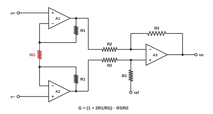
A common-mode input moves both inverting inputs together, so no current flows through \(R_{G}\) and the first stage passes it with a gain of only 1, while the differential signal is amplified by \(1 + 2R_{1}/R_{G}\). Because the gain is applied before the difference stage, the overall CMRR improves roughly in proportion to the first-stage gain. Integrated in-amps contain laser-trimmed, matched resistors on one chip; the user sets the gain with a single external \(R_{G}\).
Worked problem
Amplifying a strain gauge
The strain gauge bridge of Lesson 3 gives 1.25 mV at 500 µε. An in-amp with \(R_{1} = 25\) kΩ and \(R_{3}/R_{2} = 1\) must give 1.0 V at that strain. Find \(R_{G}\). If the in-amp's CMRR is 100 dB, what error does the 2.5 V common-mode voltage cause?
Show solution
- Required gain: \(1.0/0.00125 = 800\).
- \(1 + 50{,}000/R_{G} = 800\), so \(R_{G} = 50{,}000/799 = 62.6\) Ω.
- CMRR of 100 dB is \(10^{5}\). Referred to the input, the common-mode error is \(2.5/10^{5} = 25\) µV, about 2% of the 1.25 mV signal; at the output, \(25 \times 10^{-6} \times 800 = 20\) mV.
Answer: \(R_{G} \approx 62.6\) Ω (the nearest E96 value is 63.4 Ω, giving a gain of 790; small gain errors are removed by calibration). The common-mode error is about 2% of full scale, and since the common-mode voltage is constant, it appears as a fixed offset that is also removed by calibrating at zero strain.
Offset voltage and bias current
Real op amps produce a small output even with both inputs grounded. This is modeled by an input offset voltage \(V_{OS}\), a small DC source in series with one input, typically 1 µV to 5 mV depending on the device, and input bias currents \(I_{B}\) flowing into each input, from picoamperes for CMOS and JFET inputs to hundreds of nanoamperes for some bipolar inputs. Both errors are amplified by the circuit's noise gain, \(1 + R_{f}/R_{1}\), regardless of whether the circuit is inverting or non-inverting:
Worked problem
Offset at high gain
A non-inverting amplifier with \(R_{f} = 100\) kΩ and \(R_{1} = 1\) kΩ uses a general-purpose op amp with \(V_{OS} = 2\) mV and \(I_{B} = 50\) nA. Estimate the output error with zero input. Compare a precision op amp with \(V_{OS} = 25\) µV and \(I_{B} = 1\) nA.
Show solution
- Noise gain: \(1 + 100/1 = 101\).
- General purpose: \(101 \times 2\) mV \(+ 50 \times 10^{-9} \times 100{,}000 = 202 + 5 = 207\) mV.
- Precision: \(101 \times 25\) µV \(+ 1 \times 10^{-9} \times 100{,}000 = 2.5 + 0.1 = 2.6\) mV.
Answer: About 207 mV with the general-purpose part, enough to swamp a millivolt-level signal, against 2.6 mV with the precision part. Offset also drifts with temperature (a few µV/°C), which calibration at one temperature cannot remove. Chopper-stabilized and auto-zero op amps reduce offset and drift to below a microvolt for the most demanding measurements.
Current loops: 4–20 mA
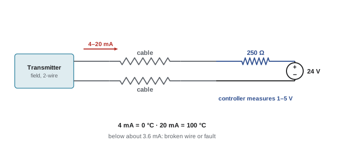
Industrial and building sensors, including the temperature, pressure, flow and humidity transmitters of data center cooling systems, commonly send their readings as a current between 4 mA and 20 mA rather than a voltage. A current signal is unaffected by the resistance of long wires, as long as the loop supply has enough voltage to drive it, and it is less susceptible to electrical noise. The "live zero" of 4 mA lets the receiver distinguish a reading of zero from a broken wire (0 mA), and lets two-wire transmitters power themselves from the loop.
Worked problem
Reading a 4–20 mA loop
A transmitter spans 0 °C to 100 °C over 4–20 mA. The controller uses a 250 Ω resistor. (a) What temperature does 12.8 mA represent, and what voltage does the controller see? (b) The loop supply is 24 V, the transmitter needs at least 10 V across it, and the cable has 2 × 15 Ω. Is the supply sufficient at 20 mA?
Show solution
- (a) \(T = (12.8 - 4)/16 \times 100 = 55\) °C; \(V = 0.0128 \times 250 = 3.2\) V.
- (b) At 20 mA: resistor \(5.0\) V, cable \(0.02 \times 30 = 0.6\) V, transmitter at least 10 V: total 15.6 V, below 24 V.
Answer: 55 °C and 3.2 V; and yes, the supply leaves 8.4 V of margin. The loop budget, the sum of all voltage drops at 20 mA, sets how long a cable and how many receivers a loop can have. Inside a transmitter, an op amp and a transistor form a voltage-to-current converter that forces the loop current to follow the sensor signal.
Comparators and hysteresis
A comparator compares two voltages and switches its output between two levels depending on which is larger: a thermostat, an over-voltage detector, a zero-crossing detector. An op amp without feedback acts as a crude comparator, but dedicated comparator chips switch faster and have outputs designed to drive logic.
A comparator fed a slowly changing, noisy signal near its threshold will switch back and forth many times as noise crosses the threshold. Hysteresis fixes this by using positive feedback to create two thresholds: the output switches high at the upper threshold and back low only at the lower one. The circuit is called a Schmitt trigger.
Worked problem
Designing hysteresis
An inverting Schmitt trigger has an op amp output that swings between +12 V and −12 V. The output feeds the non-inverting input through \(R_{2} = 100\) kΩ, with \(R_{1} = 10\) kΩ from that input to ground. Find the thresholds and the hysteresis.
Show solution
- The non-inverting input sits at \(v_{o}R_{1}/(R_{1} + R_{2}) = v_{o}/11\).
- With \(v_{o} = +12\) V: upper threshold \(+12/11 = +1.09\) V. With \(v_{o} = -12\) V: lower threshold \(-1.09\) V.
- Hysteresis: \(1.09 - (-1.09) = 2.18\) V.
Answer: Thresholds of ±1.09 V and a hysteresis of 2.18 V: noise smaller than 2.18 V peak-to-peak cannot cause repeated switching. Adding a reference voltage instead of ground at \(R_{1}\) shifts both thresholds to center them where needed. The same idea appears in every thermostat and alarm with a separate "set" and "clear" level, and in the dead band of control systems.
Analog-to-digital conversion
An analog-to-digital converter (ADC) turns a voltage into a binary number. An \(n\)-bit ADC with a full-scale range \(V_{FS}\) divides it into \(2^{n}\) steps, each one least significant bit (LSB):
The conversion can never be more accurate than ±½ LSB, the quantization error. Real ADCs add offset, gain and linearity errors, and noise. Common architectures include successive-approximation (SAR) converters, which use an internal DAC like the R-2R ladder of Lesson 3 and a comparator to find each bit in turn; sigma-delta converters, which trade speed for very high resolution (24 bits) and suit slow sensors; and flash converters, which use a resistor string and \(2^{n} - 1\) comparators to convert in a single step at very high speed.
Worked problem
From shunt to number
The UPS battery shunt of Lesson 3 (400 A at 50 mV) is amplified by a gain of 60 and read by a 12-bit ADC with a 3.3 V full scale. (a) What is the LSB in volts and in amperes? (b) What code does a 120 A discharge produce?
Show solution
- (a) LSB \(= 3.3/4096 = 0.806\) mV at the ADC. At the shunt this is \(0.806/60 = 13.4\) µV, which corresponds to \(13.4 \times 10^{-6}/0.000125 = 0.107\) A.
- (b) Shunt voltage \(120 \times 0.000125 = 15\) mV; amplified \(15 \times 60 = 900\) mV; code \(\lfloor 900/0.806 \rfloor = 1{,}117\).
Answer: Each step is about 0.11 A, and 120 A reads as code 1,117. Full scale corresponds to \(3.3/60 = 55\) mV at the shunt, or 440 A, just above the shunt's rating, a sensible match. Choosing the gain to use most of the ADC's range for the expected signal is a basic step in designing any measurement chain.
Measurement chains used for revenue metering in the US must meet ANSI C12 accuracy standards, and utility meters are regulated by state public utility commissions.
Common mistakes
MistakeUsing a simple difference amplifier with ordinary resistors for bridge signals.
InsteadUse an instrumentation amplifier with high CMRR and input resistance.
MistakeIgnoring offset voltage in high-gain DC circuits.
InsteadMultiply offset by the noise gain and choose a precision or auto-zero op amp if needed.
MistakeFeeding a slow, noisy signal to a comparator without hysteresis.
InsteadUse a Schmitt trigger with hysteresis larger than the noise.
MistakeForgetting the loop budget in 4–20 mA circuits.
InsteadAdd all voltage drops at 20 mA and compare with the loop supply.
MistakeUsing a small fraction of an ADC's range.
InsteadChoose gain so the expected signal spans most of full scale.
Summary and key terms
- Sensors often produce small differential signals on large common-mode voltages; CMRR measures rejection.
- Simple difference amplifiers are limited by resistor matching; in-amps achieve high CMRR and input resistance.
- Offset voltage and bias current are multiplied by the noise gain.
- 4–20 mA loops carry sensor signals over long wires with a live zero.
- Comparators with hysteresis (Schmitt triggers) switch cleanly on noisy signals.
- ADCs quantize voltages into codes of one LSB = V_FS/2ⁿ; gain should match the signal to the range.
- Common-mode voltage
- The average of two input voltages.
- CMRR
- Common-mode rejection ratio: differential gain divided by common-mode gain.
- Instrumentation amplifier
- A high-CMRR, high-input-resistance differential amplifier with gain set by one resistor.
- Input offset voltage
- The small differential input voltage that makes a real op amp's output nonzero.
- Noise gain
- The gain 1 + Rf/R1 applied to errors at the op amp input.
- 4–20 mA loop
- A current signaling standard for sensors.
- Live zero
- A nonzero minimum signal that distinguishes zero from a fault.
- Schmitt trigger
- A comparator with hysteresis from positive feedback.
- LSB
- Least significant bit: the smallest step of a converter.
- Quantization error
- The difference between an analog value and its digital representation, up to ±½ LSB.
Practice problems
Work each problem on paper first, then reveal the answer to check.
v+ = 2.501 V, v− = 2.499 V. Differential and common-mode voltages?
Show answer
2 mV and 2.5 V.
CMRR of 80 dB as a ratio?
Show answer
10,000.
Difference amp, G = 10, 0.1% resistors. Worst-case CMRR?
Show answer
11/(0.004) = 2,750 (about 69 dB).
In-amp with R1 = 24.7 kΩ, R3/R2 = 1. RG for a gain of 100?
Show answer
499 Ω.
Noise gain 51, VOS = 1 mV. Output offset from VOS?
Show answer
51 mV.
4–20 mA spanning 0–10 bar. Pressure at 8 mA?
Show answer
2.5 bar.
Why is 4 mA, not 0 mA, the bottom of the range?
Show answer
To detect broken wires and power two-wire transmitters.
Schmitt trigger: ±5 V output, R1 = 10 kΩ, R2 = 40 kΩ. Thresholds?
Show answer
±1 V.
16-bit ADC, 5 V full scale. LSB?
Show answer
76.3 µV.
10-bit ADC, 3.3 V. Code for 1.0 V?
Show answer
310.
Lesson quiz · 5 questions
Score 60% or more to complete this lesson.
Create a free account to save your progress, take quizzes and earn a certificate.