
CMP-315 · Lesson 4 of 12 · 21 min
GPIO and digital input and output
General-purpose input and output pins are the simplest way a microcontroller touches the world, and the most used. A GPIO pin can read whether a switch is open or closed, drive an LED or a transistor, enable a regulator, reset a modem, select a chip on a serial bus, or be handed over to a peripheral such as a UART or timer. Behind each pin is a small but important circuit, and the firmware configures it through a handful of registers. Getting that configuration wrong is the cause of many bench mysteries: an input that reads random values, an LED that glows faintly, a chip that resets itself, a microcontroller that gets warm. This lesson covers the pin circuit, input and output modes, pull resistors, drive strength, switch bouncing and the rules for connecting pins to other voltages.
On the NS-4, GPIO pins read the tamper switch on the enclosure door, drive the status LED, switch the radar module's power, control the heater relay through a transistor, hold the modem in reset, and enable the RS-485 driver. CMP-240 sized several of the resistors and capacitors around these pins. This lesson looks at the same pins from the firmware side.
Inside a GPIO pin
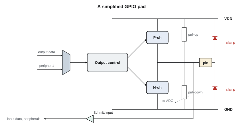
Each pin connects to a pad cell containing an output driver, an input buffer, optional pull-up and pull-down resistors, and protection diodes. The output driver is a pair of transistors: a P-channel transistor that can connect the pin to the supply, and an N-channel transistor that can connect it to ground. The input buffer is a Schmitt-trigger comparator that converts the pin voltage to a logic level with some hysteresis, so slowly changing or slightly noisy signals do not cause rapid toggling. The protection diodes clamp the pin to the supply and ground rails, which guards against brief overvoltage from static discharge but is not meant to carry continuous current. Multiplexers select whether the pin is driven by the GPIO output register or by a peripheral, and whether its input goes to the GPIO input register, a peripheral, or the analog converter.
| Mode | Output driver | Input buffer | Typical use |
|---|---|---|---|
| Input, floating | Off | On | Signal driven by another chip |
| Input with pull-up or pull-down | Off | On | Switches and buttons, open-drain signals |
| Output, push-pull | Both transistors active | On (reads back pin) | LEDs, enables, chip selects |
| Output, open-drain | N-channel only | On | Shared lines, I2C, level translation |
| Alternate function | Controlled by a peripheral | On | UART, SPI, timer, I2C pins |
| Analog | Off | Off (disconnected) | ADC and DAC pins, lowest leakage |
Inputs and the floating-pin problem
An input pin with nothing driving it is floating: its voltage drifts with leakage currents, stray capacitance and nearby signals, and the input register may read 0, 1 or flicker between them. Worse, a floating input that sits near half the supply voltage can leave both transistors of the input buffer partly on, drawing extra current, which matters greatly in a battery device. Every input must therefore have a defined level at all times, either because another chip drives it or because a pull resistor holds it. A switch to ground with a pull-up resistor reads 1 when open and 0 when closed, an inverted sense that firmware must remember. Unused pins should be configured as analog or as outputs driven low, never left as floating inputs.
Internal pull resistors are convenient but weak, typically 30 to 50 kΩ, and their value varies widely with process and temperature. They are fine for a button on a circuit board but marginal for a switch at the end of a long cable, where interference can overwhelm them. The NS-4's tamper switch is on the enclosure door, connected by 30 cm of wire, so CMP-240 used an external 47 kΩ pull-up and a 22 nF capacitor to ground, giving a time constant of about 1 ms that filters fast noise. The firmware still enables the internal pull-up as a backup and reads the pin through a debouncing routine.
Outputs: push-pull and open-drain
A push-pull output actively drives the pin both high and low. It is the normal choice for LEDs, chip selects and enables. An open-drain output can only pull the pin low or release it; a resistor, internal or external, pulls it high when released. Open-drain outputs let several devices share one line safely, because none of them ever drives high against another driving low, which is how I²C and many interrupt and reset lines work. They also allow simple level translation: an open-drain pin powered at 3.3 V, with a pull-up to 5 V, can signal to a 5 V device, provided the pin is rated as 5 V tolerant. Rise time on an open-drain line depends on the pull-up resistance and the line capacitance, which lesson 9 calculates for I²C.
Drive strength and current limits
An output pin is not an ideal voltage source. Each transistor has some on-resistance, so the output voltage sags as current flows: a pin that sources 8 mA might sit at 2.9 V instead of 3.3 V. Datasheets specify the output high and low voltages at a stated current, the maximum current per pin, and, often overlooked, the maximum total current for all pins on a port and for the whole chip. Exceeding these limits does not always destroy the chip at once, but it raises the die temperature, shifts the logic levels, adds ground bounce that disturbs other signals, and shortens the part's life. Many pins also have programmable slew rate or speed settings; a slower edge reduces ringing and electromagnetic emissions and should be used whenever the signal does not need fast edges.
Worked problem
Sizing an LED resistor and checking the pin
The NS-4 status LED is green, with a forward voltage of about 2.1 V at 4 mA. It is driven directly from a 3.3 V push-pull pin whose output-high voltage is guaranteed to be at least VDD − 0.4 V at 8 mA. Choose a series resistor for about 4 mA, and check the current if the pin's output falls to its minimum.
Show solution
- Assume the pin sits near 3.2 V at 4 mA, between the ideal 3.3 V and the guaranteed minimum.
- \[ R = \frac{3.2\ \text{V} - 2.1\ \text{V}}{4\ \text{mA}} = 275\ \Omega \;\Rightarrow\; 270\ \Omega\]
- At the guaranteed minimum of 2.9 V, the current is (2.9 − 2.1) ÷ 270 ≈ 3.0 mA.
- Both currents are well within the 8 mA per-pin rating and the LED remains visible.
Answer: Use 270 Ω. The current falls from about 4 mA to about 3 mA in the worst case, which is acceptable for a status indicator.
Loads beyond a few milliamps, such as the heater relay with its 50 mH coil, need a transistor or a dedicated driver. The pin drives the transistor's gate or base; the transistor switches the load current from a higher-voltage supply; and a flyback diode across the inductive coil, as CMP-240 explained, catches the voltage spike when the coil is switched off. The firmware sees only a pin to set and clear.
Mechanical switches bounce
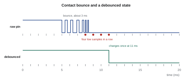
When a mechanical switch closes, its contacts do not make a single clean connection. They strike, rebound and strike again several times over a period of a few hundred microseconds to several milliseconds, so the pin sees a burst of transitions instead of one. A program that counts edges on a raw switch input will count several presses for one. Debouncing is the cure, and it can be done in hardware, in firmware or both. The hardware approach is the RC filter and Schmitt-trigger input already on the NS-4's tamper switch. The firmware approach samples the pin at a regular interval and accepts a new state only when it has been stable for several samples in a row.
# A sampled debouncer: accept a new state after N identical consecutive samples
def debounce(samples, n_stable=4, initial=1):
    state, count, last, changes = initial, 0, initial, []
    for t, s in enumerate(samples):
        if s == last:
            count += 1
        else:
            count, last = 1, s
        if count >= n_stable and s != state:
            state = s
            changes.append((t, state))
    return changes

# Raw tamper-switch samples at 1 ms: closes at t=5 with bounce, opens at t=30 with bounce
raw = [1]*5 + [0,1,0,1,0,0,1,0] + [0]*17 + [1,0,1,1,0,1] + [1]*12
edges_raw = sum(1 for a, b in zip(raw, raw[1:]) if a != b)
print("raw transitions:", edges_raw)
print("debounced changes (time ms, new state):", debounce(raw))raw transitions: 12 debounced changes (time ms, new state): [(15, 0), (38, 1)]
The raw signal changes 12 times; the debouncer reports exactly two changes, the door closing at 15 ms and opening at 38 ms, each a few milliseconds after the bouncing ends. The choice of interval and count trades responsiveness against immunity: four samples at 1 ms reject bounce up to about 3 ms long and add a delay of 4 ms, which no technician opening a door will notice. A control knob or keypad might use 5 ms samples and a count of three; a safety interlock might combine hardware filtering with a longer firmware window.
Where the firmware runs the debouncer matters too. Sampling in a periodic timer interrupt, as the NS-4 does, gives a steady interval. Using an edge-triggered interrupt on the raw switch pin is tempting but usually a mistake: the bounce generates a burst of interrupts, each costing time and energy. A common compromise is to let the first edge wake the processor from sleep and then switch to timed sampling until the state settles.
Mixed voltages and protection
Not every chip on a board runs from the same supply. The NS-4's logic runs at 3.3 V, but its radar module has 5 V signals, and the RS-485 transceiver connects to a cable that leaves the enclosure. Before connecting a pin to anything, check three numbers in both datasheets: the minimum input-high voltage of the receiver, which the driver's output-high must exceed; the maximum input-low voltage, which the driver's output-low must stay below; and the absolute maximum voltage on the receiving pin. A 3.3 V output, guaranteed at least 2.9 V high, usually satisfies a 5 V CMOS input that needs 3.5 V only if that input has TTL-compatible thresholds; otherwise a level translator is needed. In the other direction, a 5 V output must not drive a 3.3 V pin unless the pin is 5 V tolerant or a divider or translator limits the voltage, which is why CMP-240 placed a resistor divider on the radar's 5 V data output.
Signals that leave the board, such as the tamper switch wire and the RS-485 cable, need more protection: a series resistor to limit current into the clamp diodes, a transient voltage suppressor for static discharge and induced surges, and sometimes optical isolation. A pin's protection diodes can carry a few milliamps briefly; a surge from a nearby lightning strike on the pole cannot be absorbed by them. Ines added a TVS diode and a 1 kΩ series resistor to the tamper input after an NS-4 at an exposed rural site lost two pins in a thunderstorm.
Atomic pin operations and pin ownership
Lesson 3 noted that changing one bit of a register by reading, modifying and writing it is not atomic. GPIO is where that matters most, because the main loop and several interrupt handlers may change pins on the same port. If the main loop reads the output register, an interrupt handler then sets another pin on the same port, and the main loop writes back its modified value, the handler's change is silently undone. GPIO peripherals avoid this with a bit set/reset register, where writing a 1 to a bit position sets or clears that one pin and writing 0 leaves pins untouched. Some cores add bit-band aliases with the same effect. NS-4 firmware uses only the set/reset register for outputs.
Pins are also a shared resource in a subtler way. Each pin can be routed to one of several alternate functions, and the configuration must match the board. A common bring-up bug is configuring a UART's transmit pin as an alternate function but forgetting the receive pin, or choosing the wrong alternate function number, so the peripheral runs but its signals never reach the pin. Maren's rework puts every pin's configuration in a single table, generated from the schematic, and checks at start-up that no pin is claimed twice.
/* One row per pin: port, number, mode, type, pull, speed, alternate function */
static const pin_cfg_t pin_table[] = {
    { PORT_A,  5, PIN_OUTPUT,    PUSH_PULL,  PULL_NONE, SPEED_LOW,  0 },  /* status LED     */
    { PORT_A,  3, PIN_INPUT,     PUSH_PULL,  PULL_UP,   SPEED_LOW,  0 },  /* tamper switch  */
    { PORT_A,  2, PIN_ALTERNATE, PUSH_PULL,  PULL_NONE, SPEED_MED,  7 },  /* modem TX       */
    { PORT_A, 15, PIN_ALTERNATE, PUSH_PULL,  PULL_UP,   SPEED_MED,  7 },  /* modem RX       */
    { PORT_B,  6, PIN_ALTERNATE, OPEN_DRAIN, PULL_NONE, SPEED_MED,  4 },  /* I2C clock      */
    { PORT_B,  7, PIN_ALTERNATE, OPEN_DRAIN, PULL_NONE, SPEED_MED,  4 },  /* I2C data       */
    { PORT_C, 13, PIN_ANALOG,    PUSH_PULL,  PULL_NONE, SPEED_LOW,  0 },  /* unused         */
};
Common mistakes
MistakeLeaving an input pin floating.
InsteadGive every input a defined level with a driver or pull resistor, and set unused pins to analog or driven outputs.
MistakeDriving an LED or relay with no current limit or driver.
InsteadUse a series resistor for LEDs and a transistor with a flyback diode for coils; respect per-pin and total current limits.
MistakeCounting raw edges from a mechanical switch.
InsteadDebounce in hardware, firmware or both; accept a change only after the signal is stable.
MistakeConnecting a 5 V output to a pin that is not 5 V tolerant.
InsteadCheck absolute maximum ratings; use a divider, translator or tolerant pin.
MistakeUpdating outputs with read-modify-write from both the main loop and interrupts.
InsteadUse the bit set/reset register so each pin changes in a single atomic write.
Summary and key terms
- A GPIO pad contains push-pull drivers, a Schmitt-trigger input, pull resistors and clamp diodes.
- Pins can be inputs, push-pull or open-drain outputs, alternate functions or analog.
- Floating inputs read randomly and waste power; every input needs a defined level.
- Output voltage sags with current; respect per-pin and total current limits and use drivers for big loads.
- Mechanical switches bounce; sample and require several stable readings.
- Check logic thresholds and absolute maximum voltages when mixing supply voltages.
- Use set/reset registers for atomic pin changes and keep pin configuration in one table.
- GPIO
- General-purpose input and output: a pin controlled directly by firmware.
- Push-pull output
- An output that actively drives both high and low.
- Open-drain output
- An output that can only pull low; a resistor pulls the line high when released.
- Pull-up resistor
- A resistor that holds a line high when nothing drives it low.
- Schmitt trigger
- An input with hysteresis, so a slowly changing or noisy signal switches cleanly.
- Switch bounce
- Rapid repeated making and breaking of contact when a mechanical switch changes state.
- Debouncing
- Filtering switch bounce so one press is seen as one change.
- 5 V tolerant
- A pin rated to accept 5 V inputs even when the chip runs from a lower supply.
Practice problems
Work each problem on paper first, then reveal the answer to check.
A red LED has a forward voltage of 1.9 V. What resistor gives about 5 mA from a 3.3 V pin, assuming the pin sits at 3.2 V?
Show answer
(3.2 − 1.9) ÷ 5 mA = 260 Ω; use 270 Ω, giving about 4.8 mA.
A button reads 0 when pressed. Is it wired with a pull-up or a pull-down?
Show answer
A pull-up: the button connects the pin to ground when pressed.
A debouncer samples every 2 ms and requires five equal samples. What is the longest bounce it rejects, and its added delay?
Show answer
Bounce up to about 8 ms; a delay of about 10 ms after the signal settles.
Why are unused pins often set to analog mode?
Show answer
Analog mode disconnects the digital input buffer, so a floating pin draws no extra current.
Lesson quiz · 5 questions
Score 60% or more to complete this lesson.
Create a free account to save your progress, take quizzes and earn a certificate.