
ELE-210 · Lesson 12 of 12 · 22 min
Hardware description languages and programmable logic
The pedestrian controller has six states, a timer, four synchronizers, a request flag, lamp decoding and a conflict monitor. Drawn as gates, it would fill many pages, and every change would mean redrawing. Real digital design is not done that way. Designers describe hardware in a hardware description language (HDL), simulate the description to check its behavior, and let synthesis tools turn it into gates and flip-flops for a programmable chip or a custom chip. This final lesson introduces the two main HDLs, Verilog and VHDL, shows how the blocks of this course are written in Verilog, explains the difference between describing hardware and writing software, and describes the programmable devices, especially field-programmable gate arrays (FPGAs), on which most designs are first built.
Why a hardware description language?
An HDL describes the structure and behavior of a circuit as text. Text can be edited, version-controlled, reviewed, reused and, most importantly, simulated before anything is built. The same description can target an FPGA today and a custom chip next year. HDLs also let designers work at the register-transfer level (RTL): describing registers and the combinational operations between them, such as 'on each clock edge, count = count + 1 unless clear is set', and leaving the gate-level details to the tools. Writing at RTL is the main way a designer handles circuits with millions of gates.
Two HDLs dominate. Verilog, created in the mid-1980s and standardized by the IEEE, has a compact syntax somewhat like the C programming language; its extension SystemVerilog adds powerful verification features and is now the most widely used language in chip design. VHDL, developed for the US Department of Defense and also an IEEE standard, is more verbose and strongly typed, and is popular in aerospace, defense and many European organizations. A designer who knows one can read the other. The examples here use Verilog.
Describing hardware is not writing software
An HDL looks like a programming language, but its meaning is different, and confusing the two is the most common beginner's mistake. Software runs one statement after another on a processor. An HDL describes hardware in which every part operates at the same time, all the time. Two assign statements in Verilog are two pieces of logic working in parallel, not two steps. A loop in synthesizable code does not repeat over time; it replicates hardware. The test for good HDL code is simple: the designer should be able to sketch the circuit it describes, at least as blocks of registers and logic.
Only part of each language is synthesizable, meaning that a tool can turn it into hardware. Other constructs, such as delays written in nanoseconds, file input and output, and printing messages, are for simulation only. They are used in testbenches, the code that drives a design with inputs and checks its outputs, but they have no meaning in a real circuit.
Combinational logic in Verilog
A Verilog design is built from modules, each with named input and output ports. Combinational logic can be written with continuous assign statements, which describe a function of the inputs, or with an always block that is sensitive to every input, written always @(*). The walk-request function and a 4-to-1 multiplexer look like this:
module walk_request (
    input  wire p,      // pedestrian button (debounced, synchronized)
    input  wire m,      // maintenance mode
    input  wire t,      // remote test input
    output wire w
);
    assign w = (p & ~m) | t;
endmodule

module mux4 #(parameter WIDTH = 4) (
    input  wire [WIDTH-1:0] i0, i1, i2, i3,
    input  wire [1:0]       sel,
    output reg  [WIDTH-1:0] y
);
    always @(*) begin
        case (sel)
            2'b00:   y = i0;
            2'b01:   y = i1;
            2'b10:   y = i2;
            default: y = i3;
        endcase
    end
endmodule
The operators &, | and ~ are bitwise AND, OR and NOT; ^ is XOR. Buses are declared with a range such as [3:0] for four bits, and constants are written with a width and base, such as 2'b10 or 8'hD3. The parameter WIDTH makes the multiplexer reusable for any bus width. In a combinational always block, every output must be assigned for every input combination; the default branch of the case statement guarantees that. If a branch were missing, the synthesis tool would infer a latch to remember the old value, an unintended and usually harmful piece of storage. Inferred latches are one of the classic bugs that design rule checkers look for.
The seven-segment decoder
A case statement turns a truth table into code almost line for line. The tachometer's decoder from lesson 6, for a common-cathode display, is written with the segments in the order g to a. The default branch blanks the display for the illegal codes 10 to 15, a deliberate choice rather than a don't-care.
module bcd_to_7seg (
    input  wire [3:0] bcd,
    output reg  [6:0] seg      // seg[6:0] = g f e d c b a, 1 = lit
);
    always @(*) begin
        case (bcd)
            4'd0: seg = 7'b0111111;
            4'd1: seg = 7'b0000110;
            4'd2: seg = 7'b1011011;
            4'd3: seg = 7'b1001111;
            4'd4: seg = 7'b1100110;
            4'd5: seg = 7'b1101101;
            4'd6: seg = 7'b1111101;
            4'd7: seg = 7'b0000111;
            4'd8: seg = 7'b1111111;
            4'd9: seg = 7'b1101111;
            default: seg = 7'b0000000;   // blank for illegal codes
        endcase
    end
endmodule
Sequential logic in Verilog
Flip-flops are described with an always block triggered by a clock edge: always @(posedge clk). Inside such a block, assignments use the non-blocking operator <=, which means that all the right-hand sides are evaluated using the values from before the clock edge and all the registers update together, exactly like real flip-flops. Combinational blocks use the blocking operator =. Mixing them up produces simulations that do not match the synthesized hardware, so the rule is strict: <= in clocked blocks, = in combinational blocks.
module decade_counter (
    input  wire       clk,
    input  wire       rst_n,     // asynchronous reset, active low
    input  wire       en,        // count enable
    output reg  [3:0] q,
    output wire       tc         // terminal count, enables the next digit
);
    assign tc = en & (q == 4'd9);
    always @(posedge clk or negedge rst_n) begin
        if (!rst_n)
            q <= 4'd0;
        else if (en)
            q <= (q >= 4'd9) ? 4'd0 : q + 4'd1;   // illegal states also return to 0
    end
endmodule
Compare this with the decade counter of lesson 9, where the next-state equations took several lines of K-map work. Here the designer states the intended behavior and the tool derives the logic. Four instances of this module, each enabled by the terminal count of the one below, make the tachometer's four-digit BCD counter. Instantiating modules inside other modules is how hierarchy is built.
A state machine in Verilog
State machines follow a standard pattern: a state register updated on the clock, a combinational block that computes the next state, and output logic. Named constants for the states make the code readable, and the encoding can be changed by editing only the constants, or left to the synthesis tool. The pedestrian controller from lesson 10 becomes:
module ped_controller (
    input  wire clk, rst_n,
    input  wire done,          // timer expired
    input  wire car, req,      // synchronized side-street sensor and walk request
    output reg  [2:0] state,
    output wire main_g, main_y, side_g, side_y, walk, ack
);
    localparam MG = 3'd0, MY = 3'd1, AR = 3'd2, SG = 3'd3, SY = 3'd4, WK = 3'd5;
    reg [2:0] next;

    always @(posedge clk or negedge rst_n)
        if (!rst_n) state <= AR;           // start all red after reset
        else        state <= next;

    always @(*) begin
        next = state;                      // default: stay
        case (state)
            MG: if (done && (car || req)) next = MY;
            MY: if (done) next = AR;
            AR: if (done) next = req ? WK : SG;
            SG: if (done) next = SY;
            SY: if (done) next = MG;
            WK: if (done) next = MG;
            default: next = AR;            // unused codes go to all red
        endcase
    end

    assign main_g = (state == MG);
    assign main_y = (state == MY);
    assign side_g = (state == SG);
    assign side_y = (state == SY);
    assign walk   = (state == WK);
    assign ack    = (state == AR) && done && req;   // clears the request on entry to WK
endmodule
Look at the details that carry safety decisions from lesson 10 into code: reset enters the all-red state, the default branch sends unused codes to all red, and the lamp outputs depend only on the state. A separate module, deliberately written by a different engineer, implements the conflict monitor.
Testbenches and verification
Before a design is built, it is simulated. A testbench is a Verilog module with no ports that instantiates the design, generates a clock, applies input sequences and checks the outputs. Simple testbenches apply a list of input vectors and compare outputs with expected values; more advanced ones generate random inputs, check properties with assertions, such as 'main green and side green are never on together', and measure coverage to show that every state and transition has been exercised. In industry, verification usually takes more effort than design, often twice as much, because a bug found after manufacture is so expensive.
module tb_ped;
    reg clk = 0, rst_n = 0, done = 0, car = 0, req = 0;
    wire [2:0] state;
    wire mg, my, sg, sy, wk, ack;
    ped_controller dut (.clk(clk), .rst_n(rst_n), .done(done), .car(car), .req(req),
                        .state(state), .main_g(mg), .main_y(my), .side_g(sg),
                        .side_y(sy), .walk(wk), .ack(ack));
    always #5 clk = ~clk;                       // 100 MHz simulation clock
    always @(posedge clk)                       // safety assertion checked every cycle
        if ((mg || my) && (sg || sy || wk))
            $display("ERROR: conflicting signals in state %0d at %0t", state, $time);
    initial begin
        #12 rst_n = 1;
        #20 req = 1; done = 1;                  // request a walk and expire each timer
        #200 $display("final state %0d", state);
        $finish;
    end
endmodule
From PLAs to FPGAs
Programmable logic devices let a designer create custom logic without manufacturing a chip. Early devices implemented two-level logic directly. A programmable logic array (PLA) has a programmable AND plane that forms product terms and a programmable OR plane that combines them, an exact physical form of the sum of products. The programmable array logic (PAL) simplified this with a fixed OR plane, and complex programmable logic devices (CPLDs) combined many such blocks with flip-flops on one chip. These devices are still used for small glue-logic jobs, and they are why sum-of-products minimization mattered so much historically.
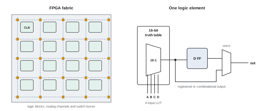
The field-programmable gate array (FPGA), introduced in the mid-1980s, took a different approach. An FPGA is a large grid of configurable logic blocks surrounded by programmable routing and input/output blocks. Each logic block contains lookup tables (LUTs) and flip-flops. A k-input LUT is a small memory of 2ᵏ bits addressed by its inputs: exactly the multiplexer-as-lookup-table of lesson 6. A 4-input LUT can implement any function of four variables, and a 6-input LUT any function of six, at the same cost and delay whatever the function. Modern FPGAs add block memories, arithmetic blocks for multiplication, high-speed serial transceivers, clock managers and sometimes whole processor cores. The configuration, called a bitstream, is loaded at power-up from a memory chip and can be changed at will, so a design can be corrected or upgraded in the field.
# Configure a 4-input lookup table: its 16 memory bits are the function's truth table
def lut_init(func):
    bits = 0
    for addr in range(16):
        d, c, b, a = (addr >> 3) & 1, (addr >> 2) & 1, (addr >> 1) & 1, addr & 1
        bits |= func(d, c, b, a) << addr
    return bits

def lut_read(init, d, c, b, a):
    return (init >> (d * 8 + c * 4 + b * 2 + a)) & 1

seg_a = lambda d, c, b, a: int(d or b or (c and a) or (not c and not a))   # from lesson 5
walk = lambda d, c, b, a: int((c and not b) or a)                          # W = P M' + T on inputs c, b, a
for name, f in (("segment a", seg_a), ("walk request", walk)):
    init = lut_init(f)
    print(f"{name:13s} LUT contents = 0x{init:04X} = {init:016b}")
print("segment a for BCD 4:", lut_read(lut_init(seg_a), 0, 1, 0, 0), " for BCD 5:", lut_read(lut_init(seg_a), 0, 1, 0, 1))segment a LUT contents = 0xFFED = 1111111111101101 walk request LUT contents = 0xBABA = 1011101010111010 segment a for BCD 4: 0 for BCD 5: 1
The LUT contents are just the output column of the truth table, read as a 16-bit number. This is why K-map minimization matters little inside an FPGA for small functions: the function segment a costs one LUT whether it is written as four product terms or sixteen minterms. Minimization still matters when it reduces the number of inputs a function needs, because a function of seven inputs needs several LUTs.
The design flow
A typical FPGA design flow runs as follows. The designer writes the specification and the RTL code. Simulation with testbenches checks the behavior. Synthesis translates the RTL into a netlist of LUTs, flip-flops and other device primitives, optimizing the logic. Place and route assigns each primitive to a physical location and connects them through the routing network. Static timing analysis checks every path against the clock constraints from lesson 11. The tools then generate the bitstream, which is loaded into the device for testing on the real board. For a custom chip, an application-specific integrated circuit (ASIC), the front of the flow is similar, but synthesis targets a library of standard cells, and the back end produces mask layouts for manufacture, with far more verification before tape-out because mistakes cannot be reprogrammed.
| Choice | FPGA | ASIC |
|---|---|---|
| Up-front cost | Low: buy devices and tools | Very high: masks and engineering can cost millions |
| Cost per unit | Higher | Lower at high volume |
| Speed and power | Good | Best: often several times faster and more efficient |
| Time to first working part | Hours to days | Months |
| Changing the design | Reprogram at any time | Requires a new chip |
| Typical use | Prototypes, low and medium volume, equipment that must be upgradable | Phones, consumer products, very high volume or very low power |
Cedarline builds its controllers on a small, low-power FPGA. The volumes are a few thousand units a year, far too few to justify a custom chip, and the ability to update the logic matters: when the city changes its signal timing rules or adds a new input, Cedarline can send a new bitstream instead of new boards. The tachometer, built in larger numbers and with a fixed function, may later move to a microcontroller with a little external logic, a decision that will weigh unit cost against flexibility.
Where to go next
This course has taken you from bits and Boolean algebra through gates, combinational blocks, arithmetic, storage, state machines, timing and HDLs. The next steps in an electrical or computer engineering program build directly on it: microcontrollers and embedded systems, where a processor executes software and digital peripherals handle timing and input/output; computer architecture, where these blocks become a processor's data path and control; and advanced digital design, which goes deeper into verification, low-power design and high-speed interfaces. Daniel's advice to Amara at the end of the project applies to every one of them: specify first, keep designs synchronous, synchronize every asynchronous input, make unused states safe, and never trust a design that has not been simulated against its specification.
Common mistakes
MistakeReading HDL code as a sequence of steps over time.
InsteadEvery assign and always block is hardware operating in parallel; loops replicate hardware.
MistakeMissing a branch in a combinational always block.
InsteadAssign every output in every case, or provide defaults, to avoid inferred latches.
MistakeUsing blocking assignments (=) in clocked blocks.
InsteadUse non-blocking (<=) in clocked blocks and blocking (=) in combinational blocks.
MistakePutting simulation-only constructs such as #delays in design code.
InsteadDelays and $display belong in testbenches; synthesis ignores or rejects them.
MistakeMinimizing small functions by hand for an FPGA.
InsteadAny function of up to k inputs uses one k-input LUT; reduce inputs, not terms.
Summary and key terms
- HDLs describe hardware as text at the register-transfer level; Verilog/SystemVerilog and VHDL are the main languages.
- HDL statements describe parallel hardware, not sequential steps; only part of each language is synthesizable.
- Combinational logic uses assign or always @(*) with every output assigned; clocked logic uses always @(posedge clk) with <=.
- Testbenches simulate designs and check them with expected values, assertions and coverage.
- PLAs and PALs implement sum-of-products directly; FPGAs use lookup tables, flip-flops and programmable routing.
- The flow runs from RTL through simulation, synthesis, place and route and timing analysis to a bitstream or masks.
- Hardware description language
- A language for describing the structure and behavior of digital hardware, such as Verilog or VHDL.
- Register-transfer level
- A design style that describes registers and the operations performed on data between them.
- Synthesis
- The automatic translation of an HDL description into a netlist of gates, flip-flops or device primitives.
- Testbench
- Simulation code that applies inputs to a design and checks its outputs.
- FPGA
- Field-programmable gate array: a chip of configurable logic blocks and routing that can be programmed after manufacture.
- Lookup table
- A small memory addressed by a function's inputs that stores its truth table, the basic logic element of an FPGA.
- Inferred latch
- Unintended storage created by synthesis when combinational code does not assign an output in every case.
Practice problems
Work each problem on paper first, then reveal the answer to check.
Write a Verilog continuous assignment for a 2-input XOR output y from inputs a and b.
Show answer
assign y = a ^ b;
What hardware does this infer: always @(*) if (en) q = d;
Show answer
A latch, because q is not assigned when en is 0.
How many memory bits does a 6-input LUT contain?
Show answer
2⁶ = 64.
Why are non-blocking assignments used in clocked always blocks?
Show answer
All right-hand sides use pre-edge values and all registers update together, matching real flip-flops.
Give the 16-bit LUT contents for a 4-input AND of D, C, B, A.
Show answer
Only address 15 is 1: 0x8000.
Name two reasons a company might choose an FPGA over an ASIC.
Show answer
Low volume (no mask costs) and the need to update the logic in the field; also faster time to market.
Lesson quiz · 5 questions
Score 60% or more to complete this lesson.
Create a free account to save your progress, take quizzes and earn a certificate.