
ELE-240 · Lesson 11 of 12 · 25 min
Single-stage amplifiers
A transistor has three terminals, and an amplifier stage uses one of them for the input, one for the output and the third as common to both, connected to signal ground. That gives three basic configurations for each type of transistor: common emitter, common base and common collector for the BJT, and common source, common gate and common drain for the MOSFET. Each has a characteristic voltage gain, input resistance and output resistance, and real amplifiers combine them, choosing each stage for the job it does best. This lesson analyzes all six with the small-signal models of lesson 10 and finishes the first stage of the pedestrian signal's microphone amplifier.
Amara's specification for that amplifier is a mid-band voltage gain of about 100 from the microphone to the envelope detector, an input resistance of at least 10 kΩ so the 2 kΩ microphone is not loaded heavily, an output that can drive the detector's 1 µF capacitor through a diode, and low enough distortion that the noise-level reading is not biased by the amplifier itself. One stage cannot meet all of that; two can.
The common-emitter amplifier
In the common-emitter (CE) amplifier, the signal enters at the base, the output is taken from the collector, and the emitter is at signal ground, either connected directly or through a bypass capacitor across R_E. The DC bias is the voltage-divider circuit of lesson 7; coupling capacitors pass the signal in and out while blocking DC. With the emitter bypassed, the small-signal analysis of lesson 10 gives
where R_B = R_1 ∥ R_2. The CE stage has high voltage gain, often a hundred or more, inverts the signal, and has moderate input and output resistances. Its weaknesses are the ones lesson 10 exposed: the gain depends on g_m, so on the bias current and temperature, and with the whole input signal across the base–emitter junction it distorts at a few millivolts.
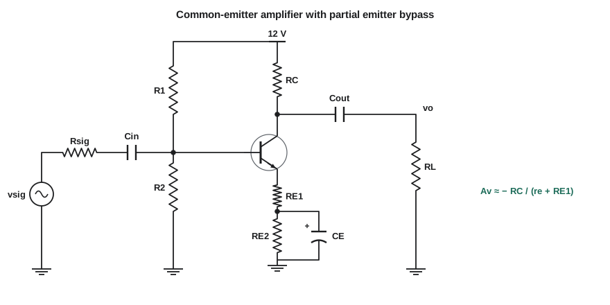
Emitter degeneration
Leaving part of the emitter resistance, R_E1, unbypassed changes the stage completely. Using the T model, the signal current in the emitter is v_b/(r_e + R_E1), and almost all of it flows in the collector, so
(neglecting r_o). When R_E1 is much larger than r_e, the gain is set by a ratio of two resistors and no longer depends on the transistor: emitter degeneration is negative feedback, and like all negative feedback it trades gain for stability, linearity and bandwidth. The input resistance rises by the factor (β + 1), because the emitter resistor appears multiplied by β + 1 when seen from the base, a rule called resistance reflection. The signal across the base–emitter junction is only a fraction r_e/(r_e + R_E1) of the input, so the stage can handle signals tens of times larger before distorting.
Worked problem
Gain-setting with partial bypass
The input stage from lesson 7 runs at I_C = 0.9 mA (r_e ≈ 28 Ω, β = 150) with R_C = 5.1 kΩ and R_B ≈ 14.8 kΩ. Its 1.5 kΩ emitter resistance is split into R_E1 = 100 Ω unbypassed and R_E2 = 1.4 kΩ bypassed. Find A_vo and R_in, and the overall gain from the 2 kΩ microphone.
Show solution
- \[A_{vo} \approx -\frac{R_C}{r_e + R_{E1}} = -\frac{5100}{28 + 100} \approx -40\]
- \[R_{in} = 14.8\ \text{k} \parallel (151 \times 128) = 14.8\ \text{k} \parallel 19.3\ \text{k} \approx 8.4\ \text{k}\Omega\]
- \[\frac{v_b}{v_{sig}} = \frac{8.4}{8.4 + 2} \approx 0.81 \quad\Rightarrow\quad \frac{v_c}{v_{sig}} \approx -40 \times 0.81 \approx -32\]
Answer: The degenerated stage gives a gain of about −40 that depends mainly on R_C/(r_e + R_E1), with an input resistance of 8.4 kΩ, a little below the 10 kΩ target. The overall gain from the microphone is about −32 before loading at the output, so a second gain stage or a larger R_C/R_E1 ratio will be needed, and raising R_1 and R_2 would lift R_in.
The common-base amplifier
In the common-base (CB) amplifier, the signal enters at the emitter, the output is taken from the collector, and the base is at signal ground. The collector current still follows the emitter current, so the voltage gain is about +g_m R_C, as large as the CE stage's and not inverted, but the input resistance looking into the emitter is only r_e, tens of ohms. The CB stage is therefore a current buffer: it accepts a current at a low impedance and delivers almost the same current at the high-impedance collector. It shines at high frequencies, because it avoids the Miller effect described in lesson 12, and in the cascode, a CE stage stacked under a CB stage, which combines high gain with wide bandwidth.
The common-collector amplifier: the emitter follower
In the common-collector (CC) amplifier, better known as the emitter follower, the signal enters at the base, the output is taken from the emitter, and the collector goes straight to the supply, which is signal ground. The emitter follows the base, one V_BE lower, so the voltage gain is just under 1. What the stage provides is impedance transformation: its input resistance is the load reflected up by β + 1, and its output resistance is the source resistance divided by β + 1, plus r_e:
Here R_L' = R_E ∥ R_L. An emitter follower lets a high-resistance source drive a low-resistance load with almost no loss: it is a voltage buffer. It is the output stage of the Zener-plus-transistor regulator of lesson 4, the output stage of many op amps and audio amplifiers, and the natural last stage of Amara's microphone amplifier, where it will drive the envelope detector.
Worked problem
Emitter follower output stage
An emitter follower biased at I_E = 2 mA (r_e = 12.5 Ω, β = 150) with R_E = 2.2 kΩ is driven from the collector of the CE stage, whose output resistance is 5.1 kΩ. It drives a 1 kΩ load. Find the gain and output resistance.
Show solution
- \[R_L' = 2.2\ \text{k} \parallel 1\ \text{k} \approx 688\ \Omega\]
- \[A_v = \frac{688}{688 + 12.5} \approx 0.98\]
- \[R_{out} \approx r_e + \frac{5100}{151} = 12.5 + 33.8 \approx 46\ \Omega \;(\parallel R_E)\]
Answer: The follower passes 98 percent of its input to the 1 kΩ load and has an output resistance of about 46 Ω. Without it, the 5.1 kΩ output of the CE stage would lose most of its signal into a 1 kΩ load.
The MOSFET configurations
The three MOSFET stages behave like their BJT counterparts, with two differences: the gate draws no current, so input resistances are set entirely by the bias network, and g_m is smaller at a given current. The common-source (CS) amplifier gives A_vo = −g_m(R_D ∥ r_o), or about −R_D/(1/g_m + R_S1) with an unbypassed source resistor, and an input resistance equal to the gate divider, which can be megohms. The common-gate (CG) stage has an input resistance of about 1/g_m and a non-inverting gain g_m R_D. The common-drain stage, the source follower, has a gain somewhat below 1, about g_m R_L'/(1 + g_m R_L'), and an output resistance of about 1/g_m, larger than an emitter follower's because g_m is smaller.
| Configuration | Voltage gain | Input resistance | Output resistance | Typical role |
|---|---|---|---|---|
| Common emitter / source | High, inverting | Moderate (BJT) / very high (MOS) | Moderate (≈ R_C) | Main gain stage |
| CE / CS with degeneration | Set by R_C / R_E1, inverting | Higher | Moderate | Stable, linear gain |
| Common base / gate | High, non-inverting | Low (≈ r_e or 1/g_m) | High | Current buffer, wideband, cascode |
| Common collector / drain | ≈ 1 (follower) | High | Low | Voltage buffer, output stage |
# Mid-band comparison of BJT stages at the same bias (IC = 1 mA, beta = 150, VA = 100 V)
VT, IC, beta, VA = 0.025, 1e-3, 150, 100.0
gm, re = IC / VT, VT / IC * beta / (beta + 1)
rpi, ro = beta / gm, VA / IC
RB, RC, RE1, RE, Rsig, RL = 15e3, 5.1e3, 100.0, 2.2e3, 2e3, 10e3
par = lambda *r: 1 / sum(1 / x for x in r)
stages = {
    "CE bypassed":   (-gm * par(RC, ro), par(RB, rpi), par(RC, ro)),
    "CE, RE1=100":   (-beta / (beta + 1) * RC / (re + RE1), par(RB, (beta + 1) * (re + RE1)), RC),
    "CB":            (gm * RC, re, RC),
    "CC follower":   (par(RE, RL) / (par(RE, RL) + re), par(RB, (beta + 1) * (re + par(RE, RL))),
                      par(RE, re + par(Rsig, RB) / (beta + 1))),
}
print(f"{'stage':14s} {'Avo':>8s} {'Rin':>10s} {'Rout':>10s} {'gain from 2k source into 10k load':>36s}")
for name, (a, rin, rout) in stages.items():
    overall = rin / (rin + Rsig) * a * RL / (RL + rout)
print(f"{name:14s} {a:8.1f} {rin:9.0f} {rout:9.0f} {overall:24.1f}")stage Avo Rin Rout gain from 2k source into 10k load CE bypassed -194.1 3000 4853 -78.4 CE, RE1=100 -40.6 8353 5100 -21.7 CB 204.0 25 5100 1.7 CC follower 1.0 14227 36 0.9
Signal swing and choosing the Q-point
An amplifier's output can swing only so far. In a CE stage the collector can rise toward V_CC as the transistor approaches cutoff, and it can fall only until the transistor saturates, about V_E + 0.3 V. For the largest symmetrical swing, the collector should sit roughly midway between those limits, taking into account that with a load connected, the signal sees R_C ∥ R_L, so the downward swing is also limited by the current available: the collector can drop by at most about I_C(R_C ∥ R_L). Daniel's rule for new designers is to calculate the swing limits in both directions and confirm that the largest expected signal fits inside both with margin.
Completing the microphone amplifier
Putting the pieces together gives Cedarline's microphone amplifier: two degenerated CE stages for gain, each giving about −10 to −15 with good linearity, followed by an emitter follower to drive the envelope detector. Two inverting stages give a non-inverted output, the gains multiply to roughly 100 to 200 after loading, and each stage's gain is set by resistor ratios rather than by β or temperature. In ELE-340 the same job would be done more elegantly with negative feedback around a multi-stage amplifier or with an op amp, but the discrete version teaches what goes on inside one.
Worked problem
Overall gain of the cascade
Stage 1 has A_vo1 = −12, R_in1 = 12 kΩ and R_out1 = 4.7 kΩ. Stage 2 has A_vo2 = −11, R_in2 = 15 kΩ and R_out2 = 4.7 kΩ. The follower has A_v3 = 0.98 and R_in3 = 120 kΩ, and its 50 Ω output drives the detector. Find the gain from the 2 kΩ microphone to the follower output.
Show solution
- \[\frac{v_1}{v_{sig}} = \frac{12}{12 + 2}(-12)\frac{15}{15 + 4.7} \approx 0.857 \times (-12) \times 0.761 \approx -7.83\]
- \[\frac{v_2}{v_1} = -11 \times \frac{120}{120 + 4.7} \approx -10.6\]
- \[\frac{v_o}{v_{sig}} \approx (-7.83)(-10.6)(0.98) \approx 81\]
Answer: The cascade gives a gain of about +81, a little short of the target of 100. Reducing R_E1 in stage 2 to raise its gain to about −14 brings the total to about 100, still with resistor-set gains and comfortable linearity.
Common mistakes
MistakeForgetting the loading of one stage by the next.
InsteadInclude R_in of the following stage, and the source and output resistances, as voltage dividers.
MistakeUsing the bypassed CE gain when part of R_E is unbypassed.
InsteadUse A ≈ −R_C/(r_e + R_E1) and R_in ≈ R_B ∥ (β+1)(r_e + R_E1).
MistakeExpecting voltage gain from an emitter follower.
InsteadIts gain is just under 1; its value is high input and low output resistance.
MistakeIgnoring the bias network in R_in.
InsteadR_1 ∥ R_2 is in parallel with the transistor's input resistance and often dominates.
Summary and key terms
- Each transistor gives three configurations: common emitter/source, common base/gate and common collector/drain.
- CE: A ≈ −g_m(R_C ∥ r_o), moderate R_in and R_out; high gain but gain set by bias and limited linearity.
- Emitter degeneration gives A ≈ −R_C/R_E1, raises R_in by (β+1) and improves linearity.
- CB/CG: low input resistance, non-inverting gain; a current buffer used in wideband and cascode stages.
- CC/CD followers: gain ≈ 1, high R_in, low R_out; voltage buffers for driving loads.
- Cascade stages and include every loading divider; check output swing in both directions.
- Common-emitter amplifier
- A BJT stage with input at the base, output at the collector and the emitter at signal ground.
- Emitter follower
- A common-collector stage whose output at the emitter follows the base with gain near 1.
- Common-base amplifier
- A BJT stage with input at the emitter, output at the collector and the base at signal ground.
- Resistance reflection
- An emitter resistance appears (β + 1) times larger when viewed from the base.
- Bypass capacitor
- A capacitor that shorts a resistor to signal ground at signal frequencies.
- Cascode
- A common-emitter (or source) stage feeding a common-base (or gate) stage, for high gain and bandwidth.
- Voltage buffer
- A stage with gain near 1, high input resistance and low output resistance.
Practice problems
Work each problem on paper first, then reveal the answer to check.
A CE stage has g_m = 40 mS, R_C = 4.7 kΩ and r_o = 100 kΩ, emitter bypassed. Find A_vo.
Show answer
−0.04 × (4.7k ∥ 100k) ≈ −0.04 × 4.49k ≈ −180.
The same stage with 220 Ω unbypassed in the emitter (r_e = 25 Ω): find A_vo.
Show answer
≈ −4700/245 ≈ −19.
Find R_in looking into the base for β = 100, r_e = 25 Ω and R_E1 = 220 Ω.
Show answer
(101)(245) ≈ 24.7 kΩ, before the bias resistors are put in parallel.
An emitter follower with r_e = 10 Ω drives R_L' = 500 Ω. Find its gain.
Show answer
500/510 ≈ 0.98.
Which configuration would you use to drive a 50 Ω cable from a 10 kΩ source?
Show answer
An emitter (or source) follower, for its low output resistance.
A source follower has g_m = 5 mS. Estimate its output resistance.
Show answer
About 1/g_m = 200 Ω.
Lesson quiz · 5 questions
Score 60% or more to complete this lesson.
Create a free account to save your progress, take quizzes and earn a certificate.