
CMP-210 · Lesson 4 of 12 · 24 min
Logic gates and CMOS
A logic gate is a circuit that computes one Boolean operation. Gates are the bricks of digital design: every combinational circuit, every flip-flop and every processor is built from them. This lesson introduces the standard gate symbols, shows that NAND and NOR gates alone can build anything, and then opens the box to show how gates are made from CMOS transistors. Knowing what is inside a gate explains its practical limits: how fast it switches, how much power it uses, how many other gates it can drive, and why its inputs must never be left floating.
Gate symbols
Each basic operation has a distinctive symbol. The AND gate has a flat input side and a round output side; the OR gate has a curved input side and a pointed output. The inverter, or NOT gate, is a triangle with a small circle, the bubble, at its output. The bubble always means inversion, so a NAND gate is an AND symbol with a bubble and a NOR gate is an OR symbol with a bubble. The XOR gate is an OR symbol with an extra curved line at the input, and XNOR adds a bubble to that. The IEEE also defines rectangular symbols with a label inside, such as & for AND and ≥1 for OR, which some schematics use.
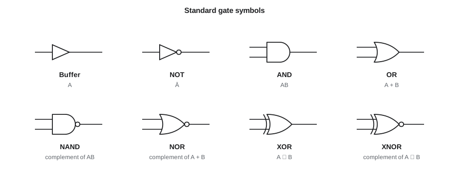
Gates with more than two inputs exist too. A 3-input AND gives 1 only when all three inputs are 1, and a 4-input NOR gives 1 only when all four are 0. In practice, gates with more than four inputs are slow in CMOS, so wide functions are built as trees of smaller gates.
| A | B | AND | OR | NAND | NOR | XOR | XNOR |
|---|---|---|---|---|---|---|---|
| 0 | 0 | 0 | 0 | 1 | 1 | 0 | 1 |
| 0 | 1 | 0 | 1 | 1 | 0 | 1 | 0 |
| 1 | 0 | 0 | 1 | 1 | 0 | 1 | 0 |
| 1 | 1 | 1 | 1 | 0 | 0 | 0 | 1 |
Universal gates
A set of gates is functionally complete if any Boolean function can be built from it. AND, OR and NOT together are complete, because every function has a sum-of-products form. Remarkably, the NAND gate alone is complete, and so is the NOR gate alone. To see this for NAND, build the three basic operations from it: tying both inputs of a NAND together makes an inverter; a NAND followed by an inverter makes an AND; and inverting both inputs of a NAND makes an OR, by De Morgan's theorem.
NAND and NOR matter because they are the natural gates of CMOS. A NAND gate uses four transistors, while an AND gate is a NAND followed by an inverter and needs six. Designers therefore like to express logic directly in NANDs and NORs. There is a neat rule for a two-level sum of products: replace every AND and the OR with NAND gates and the function is unchanged. The output OR becomes a NAND whose input bubbles cancel the bubbles of the first-level NANDs.
Worked problem
The walk-request logic in NAND gates only
Cedarline's board has spare 2-input NAND gates. Implement W = PM̄ + T using only 2-input NANDs.
Show solution
- Make M̄ with a NAND whose inputs are both M: =\overline{M \cdot M} = \overline{M}
- The SOP is an AND term (PM̄) ORed with a single literal T. Treat T as a one-variable product, which in NAND-NAND form enters the output NAND inverted.
- Make T̄ with a NAND whose inputs are both T.
- Gate 3: =X = \overline{P\overline{M}}
- Output NAND: =W = \overline{X \cdot \overline{T}} = \overline{X} + T = P\overline{M} + T
Answer: Four 2-input NANDs: one inverts M, one inverts T, one forms the complement of PM̄, and the last combines them into W.
Inside a gate: the CMOS transistor
Nearly all digital logic today is built from complementary metal-oxide-semiconductor (CMOS) technology, which pairs two kinds of field-effect transistor. An n-channel MOSFET (nMOS) conducts between its drain and source when its gate voltage is high and is off when the gate is low. A p-channel MOSFET (pMOS) does the opposite: it conducts when its gate is low and is off when the gate is high. For digital purposes each transistor is a voltage-controlled switch, and the gate draws essentially no steady current because it is insulated by a thin oxide.
A CMOS gate has two networks. The pull-up network, made of pMOS transistors, connects the output to the supply VDD when the output should be 1. The pull-down network, made of nMOS transistors, connects the output to ground when the output should be 0. The networks are designed so that for every input combination exactly one of them conducts. The output is therefore always firmly driven high or low, and, apart from brief moments during switching, there is never a path from the supply to ground.
The CMOS inverter
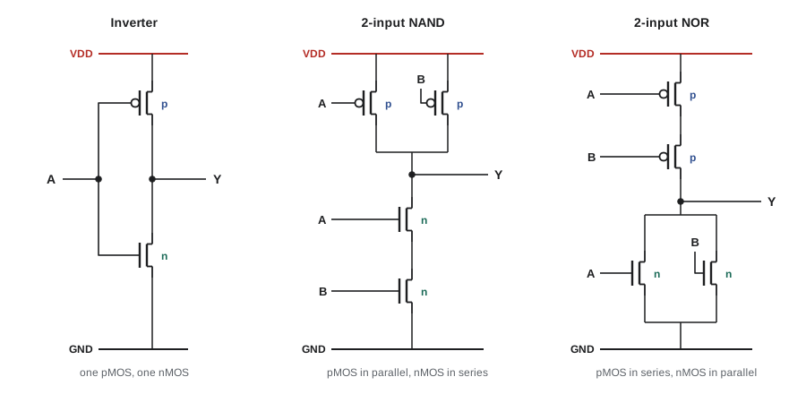
The simplest CMOS gate is the inverter: one pMOS from VDD to the output and one nMOS from the output to ground, with their gates joined as the input. When the input is low, the pMOS is on and the nMOS is off, so the output is pulled to VDD. When the input is high, the nMOS is on and the pMOS is off, so the output is pulled to ground. The voltage transfer curve, output plotted against input, is steep around the middle of the supply: a small change in input near the switching point produces a large change in output, which is what restores degraded logic levels.
CMOS NAND and NOR
For a 2-input NAND, the output must be 0 only when both inputs are 1. So the pull-down network has two nMOS transistors in series: both must be on to connect the output to ground. The pull-up network has two pMOS in parallel: if either input is 0, its pMOS conducts and the output is 1. The NOR gate is the dual: two nMOS in parallel pull the output low if either input is 1, and two pMOS in series pull it high only when both inputs are 0. This series-parallel duality is De Morgan's theorem built in silicon.
The structure explains why CMOS gates are naturally inverting: a single stage can only make a NAND, a NOR or a more complex inverting function such as AND-OR-INVERT. A non-inverting gate needs a second stage. It also explains why NAND is generally preferred to NOR. Holes in pMOS transistors are less mobile than electrons in nMOS, so pMOS transistors are weaker; a NOR gate puts the weak pMOS in series, which makes its rising output slow unless the transistors are made larger.
Noise margins
Every logic family specifies four voltages. VOH(min) is the lowest voltage a gate output guarantees for a 1, and VOL(max) is the highest it guarantees for a 0. VIH(min) is the lowest input voltage guaranteed to be read as 1, and VIL(max) is the highest guaranteed to be read as 0. The noise margins are the differences, and they say how much noise a connection can tolerate without an error.
Worked problem
Noise margins for the controller logic
The controller uses a 3.3 V CMOS family with VOH(min) = 2.4 V, VOL(max) = 0.4 V, VIH(min) = 2.0 V and VIL(max) = 0.8 V. Find the noise margins.
Show solution
- \[NM_H = 2.4 - 2.0 = 0.4\ \text{V}\]
- \[NM_L = 0.8 - 0.4 = 0.4\ \text{V}\]
- Any noise of less than 0.4 V on a connection between two gates of this family cannot cause an error.
Answer: Both noise margins are 0.4 V.
Connecting gates from different families requires checking the levels in both directions. An output that guarantees only 2.4 V for a 1 cannot reliably drive an input that needs 3.5 V, for example a 5 V CMOS part, and a 5 V output may damage a 3.3 V input unless it is designed to tolerate it. Level-shifting buffers solve both problems. Amara checks this whenever the controller talks to an older 5 V sensor module.
Fan-out, loading and propagation delay
A gate output drives the inputs of other gates and the wires between them, which together behave mostly as a capacitance. Each CMOS input adds a few picofarads in board-level parts and a fraction of a femtofarad on a chip. The output transistors must charge and discharge this capacitance on every transition, and the more load there is, the longer it takes. The fan-out of a gate is the number of inputs it drives. In CMOS, fan-out is limited by speed rather than by DC current, since the inputs draw almost no steady current.
The propagation delay is the time from an input crossing 50 per cent of the supply to the output crossing 50 per cent. Separate values are given for a rising output (tPLH) and a falling output (tPHL), and datasheets usually give typical and maximum values at a stated load. A simple but useful model treats the switching transistor as a resistance R charging the load capacitance C, giving a delay proportional to RC. Lesson 11 builds timing analysis on these delays.
Power
An ideal CMOS gate draws no current when it is not switching, which is the main reason CMOS displaced earlier technologies. Power is used when outputs change. Charging a capacitance C to VDD through the pull-up and later discharging it through the pull-down uses an energy of CV² per full cycle. With a clock frequency f and an activity factor α, the fraction of cycles in which a node switches, the dynamic power is
The square on VDD is why each new generation of chips runs from a lower supply voltage, and why phones lower their processor voltage and clock when they are idle. There is also a small short-circuit current while both transistors are briefly on during a transition, and a leakage current that flows even when nothing switches. Leakage became significant as transistors shrank and is now a major design concern in large chips.
# Noise margins and dynamic power for a small CMOS design
levels = {"VOH": 2.4, "VOL": 0.4, "VIH": 2.0, "VIL": 0.8}
nmh = levels["VOH"] - levels["VIH"]
nml = levels["VIL"] - levels["VOL"]
print(f"NM_H = {nmh:.2f} V, NM_L = {nml:.2f} V")

def p_dyn(alpha, c_farads, vdd, f_hz):
    return alpha * c_farads * vdd ** 2 * f_hz

# 2,000 nodes of 15 fF each, 10 % activity, 50 MHz clock
c_total = 2000 * 15e-15
for vdd in (3.3, 1.8, 1.2):
print(f"VDD = {vdd:3.1f} V: P = {p_dyn(0.10, c_total, vdd, 50e6) * 1e3:6.3f} mW")NM_H = 0.40 V, NM_L = 0.40 V VDD = 3.3 V: P = 1.633 mW VDD = 1.8 V: P = 0.486 mW VDD = 1.2 V: P = 0.216 mW
Practical gate outputs and inputs
Not every output is a normal push-pull output. A tri-state output has a third state, high impedance, in which both transistors are off and the output is effectively disconnected. Tri-state outputs let several devices share one bus wire, provided only one is enabled at a time. An open-drain output has only the pull-down transistor; it can pull a line low but needs an external pull-up resistor to make it high. Several open-drain outputs can share one line in a wired-AND arrangement, which is how the I²C bus and many interrupt lines work.
CMOS inputs have their own rule: never leave an unused input floating. A floating input picks up noise and can drift to the middle of the supply, where both transistors of the input stage are partly on. The gate may then oscillate, draw excess current and even overheat. Unused inputs should be tied to the supply or to ground, directly or through a resistor, as the logic requires. Push buttons, like the pedestrian button, need a pull-up or pull-down resistor so the input has a defined level when the button is open.
From gates to chips
Gates come packaged in many ways. Small-scale integrated circuits with a handful of gates, such as the classic 7400 family quad NAND, are still sold and are handy for glue logic on boards. Larger functions come as standard parts, such as counters and decoders. Most logic, however, now lives inside programmable devices (lesson 12) or custom chips, where gates are drawn from a library of standard cells and placed automatically. Whatever the packaging, the gate behaviour is the same, and the principles in this lesson apply.
Common mistakes
MistakeBuilding an AND from a single CMOS stage.
InsteadA single CMOS stage is inverting; AND is a NAND followed by an inverter.
MistakeLeaving unused CMOS inputs unconnected.
InsteadTie them high or low; floating inputs pick up noise and can oscillate.
MistakeComputing a noise margin from typical rather than guaranteed levels.
InsteadUse VOH(min) and VIH(min), VIL(max) and VOL(max).
MistakeThinking CMOS power depends mainly on the logic function.
InsteadDynamic power depends on switching activity, capacitance, frequency and the square of the supply voltage.
MistakeEnabling two tri-state drivers on one bus at the same time.
InsteadOnly one driver may be enabled; otherwise they fight and draw large currents.
Summary and key terms
- The bubble on a gate symbol means inversion; NAND and NOR are AND and OR with inverted outputs.
- NAND alone, or NOR alone, can build any Boolean function.
- A two-level AND-OR circuit converts directly into NAND-NAND.
- CMOS gates have a pMOS pull-up network and an nMOS pull-down network; series transistors in one pair with parallel ones in the other.
- Noise margins are NM_H = VOH − VIH and NM_L = VIL − VOL using guaranteed values.
- Dynamic power is αCV²f; propagation delay grows with load capacitance.
- Logic gate
- A circuit that computes one Boolean operation.
- Functionally complete
- Able to build any Boolean function, as NAND alone and NOR alone are.
- CMOS
- Complementary metal-oxide-semiconductor technology using paired pMOS and nMOS transistors.
- Pull-up network
- The pMOS transistors that connect a CMOS output to the supply.
- Propagation delay
- The time from an input crossing 50 % of the supply to the output crossing 50 %.
- Fan-out
- The number of gate inputs driven by one output.
- Tri-state output
- An output that can be high, low or disconnected (high impedance).
Practice problems
Work each problem on paper first, then reveal the answer to check.
Build a 2-input NOR gate's function using only NAND gates.
Show answer
Make Ā and B̄ with NAND inverters, NAND them to get A + B, then invert with another NAND: four NANDs.
How many transistors does a CMOS 3-input NAND use, and how are they arranged?
Show answer
Six: three pMOS in parallel from VDD to the output and three nMOS in series to ground.
A family has VOH = 4.4 V, VOL = 0.1 V, VIH = 3.5 V, VIL = 1.5 V. Find the noise margins.
Show answer
NM_H = 0.9 V and NM_L = 1.4 V.
A chip's dynamic power is 200 mW at 1.2 V and 400 MHz. Estimate it at 1.0 V and 300 MHz.
Show answer
200 × (1.0/1.2)² × (300/400) ≈ 104 mW.
Why does a push button on a CMOS input need a resistor?
Show answer
Without a pull-up or pull-down, the input floats when the button is open and its level is undefined.
Convert F = AB + CD to NAND-NAND form.
Show answer
F = NAND(NAND(A, B), NAND(C, D)).
Lesson quiz · 5 questions
Score 60% or more to complete this lesson.
Create a free account to save your progress, take quizzes and earn a certificate.