
CMP-450 · Lesson 7 of 12 · 18 min
Memories and FIFOs
Almost every FPGA design is organized around memories. They hold sample histories, coefficients, frame buffers, lookup tables and packet data, and in the form of first-in, first-out buffers (FIFOs) they connect blocks that produce and consume data at different rates or at different times. This lesson explains how to write memories that synthesis maps onto block RAM and distributed RAM, what the different read behaviors mean, how to design a synchronous FIFO correctly, and how to calculate how deep a FIFO must be.
The NS-5 front end has five memories: the four-channel sample history the filter reads, the coefficient table, two frame buffers that alternate between being filled and being read, the FIFO between the frame buffers and the direct memory access (DMA) engine that writes frames into the processor's memory, and the clock-crossing FIFO from the ADC domain, which lesson 8 builds. Jonah has to size each one and code it so that it maps onto the right resource.
Choosing the memory resource
An FPGA offers three places to store data. Flip-flops suit a few registers that must all be readable at once. Distributed RAM, built from LUTs, suits small memories of up to a few hundred words, especially when an asynchronous read is needed or when many small memories are required. Block RAM suits anything larger: each 36 Kbit block is cheap compared with the thousands of LUTs that the same memory would need as distributed RAM, and it has two full ports. The boundary is blurry, and synthesis tools choose automatically based on size, but a designer should know which resource each memory will use and can force the choice with an attribute when needed.
| Memory | Size | Resource | Reason |
|---|---|---|---|
| Sample history | 4 channels × 64 × 12 bits | distributed RAM, about 100 LUTs | small; two read addresses per cycle for the symmetric pairs |
| Coefficients | 16 × 16 bits (half, by symmetry) | LUT ROM, 16 LUTs | tiny and constant |
| Frame buffers | 2 × 4 × 1,024 × 16 bits = 128 Kbit | 4 block RAMs | large; written by the filter, read by the DMA |
| DMA FIFO | 256 × 32 bits | 1 block RAM (half used) | depth from the stall analysis below |
| ADC crossing FIFO | 512 × 48 bits | 1 block RAM | two clocks; lesson 8 |
The sample history is a circular buffer: each channel's samples are written at an advancing pointer, and the filter reads the two samples of each symmetric pair at offsets from it. Its 64 entries per channel, rather than 32, leave room for new samples to arrive while the previous output is being computed. Because every tap is read by address rather than shifted, the history cannot be a shift register; it is a small RAM with one write port and two read ports, which distributed RAM provides by duplicating the storage.
Inferring block RAM
Block RAM is inferred from an array declaration and a clocked process that writes it and reads it with a registered address or registered data. The template matters: if the read is not synchronous, the memory cannot use block RAM. The listing shows a simple dual-port RAM, one write port and one read port, each with its own clock, which is what the frame buffers use.
module sdp_ram #(
    parameter int AW = 11,                 // 2,048 words
    parameter int DW = 16,
    parameter bit OUT_REG = 1              // extra output register for speed
) (
    input  logic          wclk, we,
    input  logic [AW-1:0] waddr,
    input  logic [DW-1:0] wdata,
    input  logic          rclk, re,
    input  logic [AW-1:0] raddr,
    output logic [DW-1:0] rdata
);
    logic [DW-1:0] mem [2**AW];
    logic [DW-1:0] q;

    always_ff @(posedge wclk)
        if (we) mem[waddr] <= wdata;

    always_ff @(posedge rclk)
        if (re) q <= mem[raddr];           // synchronous read: maps to block RAM

    if (OUT_REG) begin : g_oreg
        always_ff @(posedge rclk) rdata <= q;   // read latency 2
    end else begin : g_noreg
        assign rdata = q;                        // read latency 1
    end
endmodule
The optional output register uses the register built into the block RAM's output. Without it, the clock-to-output delay of the memory array is long, often around 1.5 to 2 ns, and it adds directly to whatever logic follows. With it, the read latency becomes two cycles but the output path is as fast as a flip-flop's. At 100 MHz either works for the NS-5; at higher rates the output register is almost always enabled, and the logic that consumes the data must be designed for two cycles of latency.
Read-during-write behavior
When one port writes an address in the same cycle that a read of the same address occurs, the result depends on the memory's read-during-write mode. On the same port, read-first returns the old contents, write-first returns the new data, and no-change keeps the output at its previous value. Across two ports with different clocks, the result of a collision is undefined: the read may return old data, new data or a mixture. The HDL template determines the mode for same-port collisions: a non-blocking write and read of the same array in one block gives read-first, while code that bypasses the new data to the output gives write-first.
Designs should avoid depending on cross-port collisions. The NS-5 frame buffers are safe by construction because they are used as a ping-pong pair: while the filter writes frame k into one buffer, the DMA reads frame k − 1 from the other, and they swap at the end of each frame, so the two ports never touch the same buffer at the same time. The capture controller's done event is what swaps them.
Initialization, ROMs and memory files
Block RAM and distributed RAM contents can be initialized in the bitstream, which is how ROMs are built: an array with an initial block that loads it with $readmemh, or a case statement mapping addresses to constants, is synthesized into a memory whose contents are fixed at configuration. The NS-5 coefficients are generated by the Python model of lesson 6 into a hex file, read by both the RTL and the testbench, so the hardware and its reference can never disagree about them. Initialization is also the reason that FPGA designs can contain lookup tables for functions such as sine, logarithm and reciprocal that would be expensive to compute.
Memory bandwidth and organization
A block RAM port moves one word per cycle. When a design needs more bandwidth than a port provides, it widens the word, uses both ports, or splits the data across several memories so that they can be accessed in parallel, a technique called banking or array partitioning. The NS-5 filter needs two history samples per cycle; the distributed RAM's two read ports provide them. A filter running at the full input rate with all 16 symmetric pairs read at once would need the history in registers or split across 16 memories. Memory organization is often the real constraint on an FPGA architecture, and lesson 11 shows how high-level synthesis tools expose it.
Large memories also need error protection when reliability matters. Block RAMs typically include optional error-correcting code (ECC) logic for 64-bit words, which corrects single-bit errors and detects double-bit errors caused by radiation-induced upsets. The configuration memory itself can suffer upsets, and most devices provide a background scrubbing function that detects and corrects them. For a roadside sensor at ground level, upset rates are low, but over a fleet of thousands of units running for years they are not negligible, and lesson 12 returns to the point.
FIFOs
A FIFO is a memory with a write pointer and a read pointer, organized as a ring. Writing stores data at the write pointer and advances it; reading returns data at the read pointer and advances it. The difficulty is distinguishing full from empty, because in both cases the pointers are equal. The standard solution is to make each pointer one bit wider than the address: the low bits address the memory, and the extra top bit toggles every time the pointer wraps. The FIFO is empty when the pointers are identical, and full when their address bits match but their top bits differ, meaning the writer has lapped the reader exactly once.
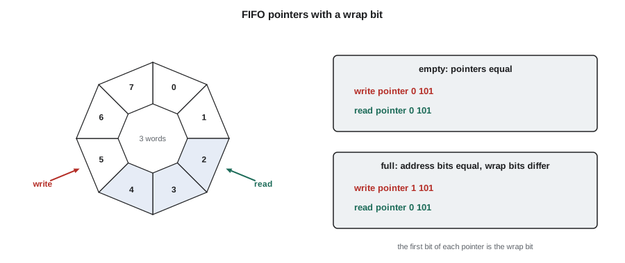
module sync_fifo #(parameter int DW = 32, parameter int AW = 8) (   // 256 deep
    input  logic          clk, rst,
    input  logic          wr, rd,
    input  logic [DW-1:0] din,
    output logic [DW-1:0] dout,
    output logic          full, empty,
    output logic [AW:0]   count
);
    logic [DW-1:0] mem [2**AW];
    logic [AW:0]   wp, rp;                    // one extra wrap bit
    logic          do_wr, do_rd;

    assign do_wr = wr && !full;               // ignore writes when full
    assign do_rd = rd && !empty;              // ignore reads when empty
    assign empty = (wp == rp);
    assign full  = (wp[AW-1:0] == rp[AW-1:0]) && (wp[AW] != rp[AW]);
    assign count = wp - rp;                   // modular subtraction

    always_ff @(posedge clk) begin
        if (rst) begin
            wp <= '0;  rp <= '0;
        end else begin
            if (do_wr) wp <= wp + 1'b1;
            if (do_rd) rp <= rp + 1'b1;
        end
        if (do_wr) mem[wp[AW-1:0]] <= din;
        if (do_rd) dout <= mem[rp[AW-1:0]];   // standard mode: data one cycle after rd
    end
endmodule
The FIFO in the listing is in standard mode: data appears one cycle after the read request. A first-word fall-through FIFO instead presents the oldest word on its output whenever it is not empty, so a reader can see the data before deciding to read it, which is exactly what a valid and ready streaming interface needs. It is built from a standard FIFO plus a small output register stage that prefetches the next word. The count output gives the occupancy, from which almost-full and almost-empty flags are derived; an almost-full flag that rises a few entries before full gives an upstream block with a pipeline delay time to stop.
Two protection rules in the listing are easy to forget. Writes when full and reads when empty are ignored rather than corrupting the pointers, and the condition is checked inside the FIFO rather than trusted to the caller. In verification, an assertion that wr is never asserted when full, and a cover property that full actually occurs, show both that the protection works and that the testbench reached the boundary.
How deep must a FIFO be?
A FIFO absorbs the difference between when data arrives and when it can leave. Its depth must cover the largest backlog that can build up, which depends on the rates and on how long the consumer can be unavailable. Two cases cover most designs. When a producer writes a burst of B words at rate f_w while the consumer reads at a lower rate f_r, the backlog at the end of the burst is:
When a producer writes steadily at rate r and the consumer can stall for up to t_stall, then drains in bursts of b words, the depth must cover the data arriving during the stall plus one burst:
Both are bounds on the worst case, not the average, and both depend on numbers that must come from somewhere real. For the NS-5, the 150 µs stall is the longest time the processor system's memory interconnect has been measured to refuse the front end's DMA while the processor writes a log block to flash, from Maren Holt's tests on the evaluation board, with a margin. The code computes both cases and checks them by simulation.
import random
from math import ceil, log2

def pow2(n):
    return 1 << ceil(log2(n))

# case 1: steady producer, bursty consumer that can be stalled
rate_w = 1.0e6          # words per second from the frame packer (two 16-bit samples per word)
stall = 150e-6          # longest time the memory interconnect refuses the DMA
burst = 64              # DMA moves data in bursts of 64 words
need1 = ceil(rate_w * stall) + burst
print(f"case 1: {rate_w * stall:.0f} words arrive during a stall, plus one burst of {burst}"
      f" -> depth >= {need1}, use {pow2(need1)}")

# case 2: burst producer, slower steady consumer
B, fw, fr = 1024, 100e6, 25e6   # 1,024-word burst written at 100 MHz, read at 25 MHz
need2 = ceil(B * (1 - fr / fw))
print(f"case 2: B(1 - fr/fw) = {B} x (1 - {fr/1e6:.0f}/{fw/1e6:.0f}) = {need2}"
      f" -> use {pow2(need2)}")

# check case 2 by simulation on the 100 MHz clock: one read every 4 cycles
occ, peak = 0, 0
for cyc in range(4 * B):
    if cyc < B:
        occ += 1                     # write
    if cyc % 4 == 3 and occ:
        occ -= 1                     # read at a quarter of the rate
    peak = max(peak, occ)
print(f"case 2 simulated peak occupancy: {peak}")

# check case 1 with random stalls over many frames, on a 100 MHz clock
random.seed(7)
occ, peak, cyc = 0, 0, 0
stall_left, granted_burst = 0, 0
for cyc in range(2_000_000):                    # 20 ms of operation
    if cyc % 100 == 0:
        occ += 1                                # one word per microsecond
    if stall_left:
        stall_left -= 1
    elif random.random() < 1e-5:
        stall_left = random.randint(1, 15_000)  # a stall of up to 150 us
    elif occ >= burst or (granted_burst and occ):   # a burst starts when 64 words wait
        granted_burst = 1
        occ -= 1                                # and moves one word per cycle until empty
        if occ == 0:
            granted_burst = 0
    peak = max(peak, occ)
print(f"case 1 simulated peak occupancy over 20 ms with random stalls: {peak} of {pow2(need1)}")case 1: 150 words arrive during a stall, plus one burst of 64 -> depth >= 214, use 256 case 2: B(1 - fr/fw) = 1024 x (1 - 25/100) = 768 -> use 1024 case 2 simulated peak occupancy: 768 case 1 simulated peak occupancy over 20 ms with random stalls: 201 of 256
For the DMA FIFO, 150 words arrive during the longest stall and one burst of 64 must fit, so the FIFO needs at least 214 entries and is built with 256, which with 32-bit words uses half of one block RAM. The random-stall simulation over 20 ms peaks at 201 entries. For the burst case, the formula gives exactly the simulated peak of 768, and the FIFO is made 1,024 deep. Rounding up to a power of two keeps the pointer logic simple and, for clock-crossing FIFOs, is required by the Gray-code pointers of lesson 8.
A FIFO that is too shallow does not fail politely: it overflows, and data is lost. The NS-5 design therefore treats overflow as an error to be detected and reported, never as a normal condition. The DMA FIFO has a sticky overflow flag in the status register, and the frame header records the FIFO's peak occupancy, so that Dev Okafor's field logs will show whether real stalls ever come close to the design limit.
Common mistakes
MistakeWriting a memory with an asynchronous read and expecting block RAM.
InsteadRegister the read address or data so the memory maps to block RAM.
MistakeForgetting the extra cycle of latency from the block RAM output register.
InsteadDesign the consumer for the chosen read latency of one or two cycles.
MistakeRelying on the result of a read and write to the same address from two ports.
InsteadStructure the design, for example as ping-pong buffers, so collisions cannot happen.
MistakeDistinguishing full from empty with a separate counter that can drift out of step.
InsteadUse pointers one bit wider than the address and compare them.
MistakeSizing a FIFO from average rates.
InsteadSize it from the worst-case burst or stall and verify the peak occupancy by simulation.
Summary and key terms
- Flip-flops, distributed RAM and block RAM suit different sizes and access patterns.
- Block RAM needs a synchronous read; its optional output register gives two cycles of latency and a fast output.
- Same-port read-during-write behavior is set by the template; cross-port collisions are undefined.
- Memories can be initialized from files, which is how ROMs and lookup tables are built.
- A FIFO with pointers one bit wider than the address is empty when they are equal and full when only the top bits differ.
- FIFO depth follows from B(1 − f_r/f_w) for bursts or r t_stall + b for stalls; the NS-5 DMA FIFO needs 214 and uses 256.
- Distributed RAM
- Memory built from LUTs, suited to small sizes and asynchronous reads.
- Simple dual-port RAM
- A memory with one write port and one read port, which may use different clocks.
- Read-during-write mode
- The behavior of a memory read that occurs in the same cycle as a write to the same address.
- Ping-pong buffer
- A pair of buffers used alternately, one being filled while the other is read.
- FIFO
- A first-in, first-out buffer built from a memory and read and write pointers.
- First-word fall-through
- A FIFO mode in which the oldest word is visible at the output before it is read.
- Almost-full flag
- A flag that warns a writer before a FIFO is completely full.
- Banking
- Splitting data across several memories so they can be accessed in parallel.
Practice problems
Work each problem on paper first, then reveal the answer to check.
How many 36 Kbit block RAMs does a 4,096 × 32 memory need?
Show answer
Using 1K × 36, four blocks deep; 4 blocks.
A FIFO receives a burst of 512 words at 200 MHz and is read at 50 MHz. What depth is needed?
Show answer
512 × (1 − 50/200) = 384, so 512 in practice.
With AW = 3, the write pointer is 1010 and the read pointer is 0010. Is the FIFO full, empty or neither?
Show answer
Address bits 010 match and the top bits differ, so it is full.
Why does the sample history use 64 entries per channel when the filter has 32 taps?
Show answer
So that new samples can be written while the current output is still reading the previous 32, without overwriting them.
Lesson quiz · 5 questions
Score 60% or more to complete this lesson.
Create a free account to save your progress, take quizzes and earn a certificate.