
CMP-450 · Lesson 10 of 12 · 22 min
Interfaces: UART, SPI, AXI-style streaming handshakes, video timing
An FPGA is useful only to the extent that it talks to the rest of the system, and most FPGA projects spend as much effort on interfaces as on processing. This lesson builds four of them in the forms they take inside the NS-5 front end: a UART for the debug console, an SPI master that configures the ADC, the valid and ready streaming handshake that connects every block in the data path, and the video timing generator that drives a monitor on the lab's bench-test rig. Each one illustrates a different aspect of interface design: asynchronous sampling, generated clocks, flow control and precise timing.
The embedded systems course covered UART and SPI from the microcontroller side, as peripherals configured by registers. Here you build the peripherals themselves, which means deciding exactly what happens on every clock cycle.
UART
A UART sends each byte as a frame: a start bit at 0, eight data bits least significant first, and a stop bit at 1, the format called 8N1. There is no clock line; the transmitter and receiver agree on a bit rate, and the receiver recovers timing from the falling edge of each start bit. A transmitter is a simple state machine driven by a bit-rate tick from a counter: it loads a 10-bit shift register with the frame and shifts one bit out per tick.
module uart_tx #(parameter int CLK_HZ = 100_000_000, parameter int BAUD = 115_200) (
    input  logic       clk, rst,
    input  logic       valid,          // stream input: byte to send
    output logic       ready,
    input  logic [7:0] data,
    output logic       txd
);
    localparam int DIV = (CLK_HZ + BAUD / 2) / BAUD;   // 868 clocks per bit, rounded
    logic [$clog2(DIV)-1:0] tick_cnt;
    logic [9:0] sh;                    // stop, data[7:0], start
    logic [3:0] bits;                  // bits left to send

    assign ready = (bits == 0);
    always_ff @(posedge clk) begin
        if (rst) begin
            bits <= '0;  txd <= 1'b1;  tick_cnt <= '0;
        end else if (bits == 0) begin
            txd <= 1'b1;               // idle line is high
            if (valid) begin
                sh <= {1'b1, data, 1'b0};
                bits <= 4'd10;  tick_cnt <= '0;
            end
        end else if (tick_cnt == DIV - 1) begin
            tick_cnt <= '0;
            txd  <= sh[0];
            sh   <= sh >> 1;
            bits <= bits - 1'b1;
        end else
            tick_cnt <= tick_cnt + 1'b1;
    end
endmodule
The receiver is harder because its input is asynchronous. The rx pin first passes through the two-flip-flop synchronizer of lesson 8; the constraint file of lesson 9 declares the pin a false path for exactly this reason. The receiver then samples the line at 16 times the bit rate. When it sees the line low, it waits eight sample ticks to reach the middle of the start bit, checks that the line is still low, which rejects short glitches, and then samples each data bit 16 ticks later, in the middle of the bit. Sampling in the middle gives the largest tolerance to rate mismatch between the two ends.
That tolerance can be calculated. Over a frame, the receiver's sampling point drifts relative to the transmitter's bits by the rate mismatch times the elapsed time. The last sample, in the middle of the stop bit, is 9.5 bit times after the start edge, and it must still fall within the stop bit, so the drift must be less than half a bit: a total mismatch of 0.5/9.5, or about 5.3 %, shared between the two ends, and in practice less because of the sampling granularity and edge distortion. Each end should therefore be within about 2 % of the nominal rate.
import random

# UART: divisor for 16x oversampling from the 100 MHz system clock
F = 100e6
for baud in (9600, 115200, 921600):
    div = round(F / (16 * baud))
    actual = F / (16 * div)
    print(f"UART {baud:7d} baud: divisor {div:4d}, actual {actual:9.1f}, error {100 * (actual / baud - 1):+.2f} %")
# a receiver samples each bit at its middle; by the stop bit (bit 9.5 of a 10-bit frame)
# the accumulated mismatch must stay under half a bit, shared between the two ends
print(f"tolerable total mismatch for 8N1: {100 * 0.5 / 9.5:.1f} %")

# video timing for 640 x 480 at nominally 60 Hz
h = dict(active=640, front=16, sync=96, back=48)
v = dict(active=480, front=10, sync=2, back=33)
ht, vt = sum(h.values()), sum(v.values())
for pclk in (25.175e6, 25.0e6):
    print(f"pixel clock {pclk/1e6:.3f} MHz: line {ht} clocks = {ht / pclk * 1e6:.3f} us, "
          f"frame {ht} x {vt}, refresh {pclk / (ht * vt):.2f} Hz")

# valid/ready: a naive registered stage versus a skid buffer, with random backpressure
def run(stage, cycles=100_000, p_ready=0.8, seed=10):
    rnd = random.Random(seed)
    sent = 0
    buf = []                                  # data held inside the stage
    cap = 1 if stage == "naive" else 2
    for _ in range(cycles):
        ready_out = rnd.random() < p_ready    # downstream sink
        # the stage's ready output is a register: it depends only on the state at the
        # start of the cycle, not on this cycle's ready_out
        if stage == "naive":
            ready_in = len(buf) == 0          # accepts only when empty
        else:
            ready_in = len(buf) < cap         # skid register absorbs one extra word
        if buf and ready_out:
            buf.pop(0); sent += 1             # output transfer
        if ready_in:                          # the source always has data
            buf.append(1)
    return sent / cycles

for st in ("naive", "skid"):
print(f"{st:5s} registered stage, sink ready 80 % of cycles: throughput {run(st):.3f} words/cycle")UART 9600 baud: divisor 651, actual 9600.6, error +0.01 % UART 115200 baud: divisor 54, actual 115740.7, error +0.47 % UART 921600 baud: divisor 7, actual 892857.1, error -3.12 % tolerable total mismatch for 8N1: 5.3 % pixel clock 25.175 MHz: line 800 clocks = 31.778 us, frame 800 x 525, refresh 59.94 Hz pixel clock 25.000 MHz: line 800 clocks = 32.000 us, frame 800 x 525, refresh 59.52 Hz naive registered stage, sink ready 80 % of cycles: throughput 0.444 words/cycle skid registered stage, sink ready 80 % of cycles: throughput 0.800 words/cycle
With 16-times oversampling from the 100 MHz system clock, 115,200 baud needs a divisor of 54.25, rounded to 54, an error of +0.47 %, comfortably within budget. At 921,600 baud the divisor is about 6.8 and must be 7, an error of −3.12 %, which risks failures against a host that is itself slightly off. The fixes are a lower oversampling ratio, a fractional divisor that alternates between two values, or a clock frequency chosen for serial rates. The NS-5 debug console runs at 115,200 baud, which is what Dev Okafor's field laptop expects.
SPI
SPI is a synchronous serial interface with a master that drives a clock (SCLK), a chip select (CS, active low), master-out data (MOSI) and receives master-in data (MISO). Four modes, set by clock polarity (CPOL) and phase (CPHA), define which edge launches data and which samples it; mode 0, the most common, idles the clock low, samples on the rising edge and changes data on the falling edge. The NS-5 ADC uses mode 0 with 24-bit transactions: a read or write bit, a 7-bit register address, a pad, and 16 bits of data.
An SPI master in an FPGA should not generate SCLK by toggling a register on a divided clock and then use that SCLK to clock its own logic. Instead, everything runs on the system clock, and SCLK is an output register that toggles under a clock enable every two system cycles for a 25 MHz SCLK. MOSI changes and MISO is sampled on the system clock cycles that correspond to the SCLK falling and rising edges. This keeps the whole interface in one clock domain, and the timing at the pins is checked by STA through the generated-clock and output-delay constraints of lesson 9. The round trip to the ADC and back also matters: MISO data launched by the ADC on a falling SCLK edge must return through the board and input buffers before the master samples it, which limits SCLK to well below the system clock in most designs.
Worked problem
SPI round-trip timing
The ADC changes MISO up to 12 ns after the falling SCLK edge. Board traces add 1 ns in each direction, and the FPGA input path and setup need 3 ns. The master samples MISO one half SCLK period after the falling edge. What is the highest SCLK frequency?
Show solution
- The data must arrive within half a period of the falling edge at the FPGA's SCLK output.
- \[ t_{trace,out} + t_{co,ADC} + t_{trace,in} + t_{in} = 1 + 12 + 1 + 3 = 17 \text{ ns} \le \frac{T_{SCLK}}{2}\]
- \[ T_{SCLK} \ge 34 \text{ ns} \;\to\; f_{SCLK} \le 29.4 \text{ MHz}\]
- A 25 MHz SCLK, from the system clock divided by four, leaves 3 ns of margin. Sampling a full period later instead, which some masters allow, would double the limit.
Answer: About 29 MHz, so 25 MHz is used.
Streaming handshakes
Inside the front end, every block passes data to the next through the same simple protocol, modeled on the AXI4-Stream interface of the AMBA family of on-chip bus standards and used, under various names, by almost every FPGA design team. The source drives data and a valid signal; the sink drives a ready signal; a transfer happens on every clock edge where both valid and ready are high. Optional sideband signals include last, marking the final word of a packet or frame, and keep or user fields with byte enables or metadata. The NS-5 uses last to mark the end of each 1,024-sample frame and a user field to carry the channel number.
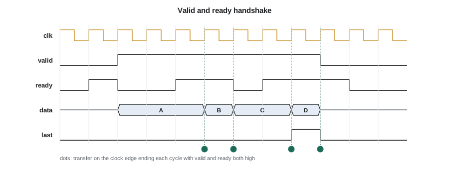
The rules are few and strict. A source must not wait for ready before asserting valid, because a sink is allowed to wait for valid before asserting ready, and if both waited the system would deadlock. Once valid is asserted, it must stay asserted, with the data unchanged, until the transfer happens. A sink may assert or remove ready at any time. These are exactly the properties the assertions of lesson 4 check on every interface.
The handshake gives every block flow control for free. When the DMA engine is stalled, as in the FIFO analysis of lesson 7, it lowers ready; the FIFO fills; when the FIFO is full, it lowers its own ready; and the stall propagates backward through the pipeline to wherever the data can be held. Blocks that cannot stop, such as the ADC capture, sit behind a FIFO deep enough for the worst stall, and raise an overflow error if it ever fills.
Pipelining a handshake: the skid buffer
Ready travels backward through a pipeline, against the data. If each stage simply passes ready through combinationally, a long chain of stages forms a long combinational path from the last sink to the first source, which fails timing exactly as lesson 9 described. Registering ready breaks the path but introduces a cycle of delay: when the sink drops ready, the stage only learns about it a cycle later and has already accepted one more word, which it must store somewhere. A naive registered stage avoids the problem by accepting a new word only when it is empty, which halves its throughput. The skid buffer solves it properly by adding a second register that catches the one extra word.
module skid_buffer #(parameter int W = 32) (
    input  logic         clk, rst,
    input  logic         s_valid,  output logic s_ready,  input  logic [W-1:0] s_data,
    output logic         m_valid,  input  logic m_ready,  output logic [W-1:0] m_data
);
    logic         skid_valid;
    logic [W-1:0] skid_data;

    assign s_ready = !skid_valid;              // registered: depends only on state

    always_ff @(posedge clk) begin
        if (rst) begin
            m_valid <= 1'b0;  skid_valid <= 1'b0;
        end else begin
            if (m_ready || !m_valid) begin       // output register can take a word
                if (skid_valid) begin            // drain the skid register first
                    m_data  <= skid_data;  m_valid <= 1'b1;  skid_valid <= 1'b0;
                end else begin
                    m_data  <= s_data;     m_valid <= s_valid;
                end
            end else if (s_valid && s_ready) begin
                skid_data <= s_data;  skid_valid <= 1'b1;   // catch the extra word
            end
        end
    end
endmodule
The simulation in the code block above compares the two designs with a sink that is ready on a random 80 % of cycles. The naive stage achieves 0.444 words per cycle; the skid buffer achieves 0.800, the full rate the sink allows. The skid buffer costs one extra register of data width, and it is the standard way to insert pipeline registers into any valid and ready path, including the ones the timing fixes of lesson 9 require.
Video timing
A display interface sends pixels in a fixed raster: each line is a period of active pixels followed by a horizontal blanking interval containing a front porch, a sync pulse and a back porch, and each frame is a set of active lines followed by a vertical blanking interval made the same way, counted in lines. The widely used 640 × 480 mode at about 60 Hz has 800 pixel clocks per line (640 active, 16 front porch, 96 sync, 48 back porch) and 525 lines per frame (480 active, 10, 2 and 33), with negative sync polarity and a nominal 25.175 MHz pixel clock.
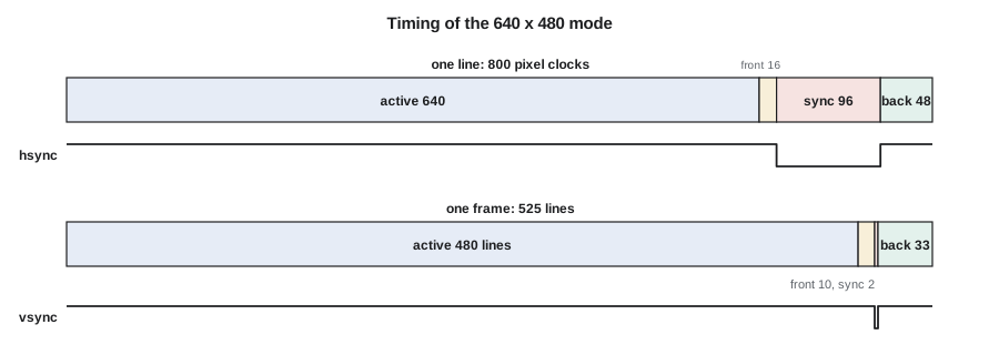
The timing generator is two counters: a horizontal counter from 0 to 799 at the pixel clock, and a vertical counter from 0 to 524 that advances when the horizontal counter wraps. The sync outputs and an active-video flag are simple comparisons of the counters, registered so that they change cleanly on clock edges. The code block above shows that a 25.0 MHz pixel clock, obtained by dividing the 100 MHz system clock by four with a clock enable, gives 59.52 Hz instead of 59.94 Hz, which nearly all monitors accept. The bench-test build uses this to draw the four channels' filtered samples as live traces, which has been Jonah's most useful debugging tool.
// pixel-rate enable: one cycle in four of the 100 MHz clock gives 25 MHz
always_ff @(posedge clk) begin
    if (pix_en) begin
        if (h == 10'd799) begin
            h <= '0;
            v <= (v == 10'd524) ? '0 : v + 1'b1;
        end else
            h <= h + 1'b1;
        hsync  <= !(h >= 10'd655 && h < 10'd751);   // 640 + 16 to 640 + 16 + 96, one cycle early
        vsync  <= !(v >= 10'd490 && v < 10'd492);   // 480 + 10 to 480 + 10 + 2
        active <= (h < 10'd640) && (v < 10'd480);   // lines up with pixel data, also registered once
    end
end
The sync comparison values in the listing are offset by one because hsync is registered: it is computed from the counter value of the current pixel but appears at the output one pixel later, a typical piece of pipeline bookkeeping. Because the outputs are registered, all the video signals change on the same edge and arrive at the connector aligned with each other, which is what the monitor needs.
Interfaces as contracts
Each interface in this lesson is a contract between two parties with different timing: a host computer, an ADC, another block, a monitor. Good interface design writes that contract down, in a timing diagram, a register map or a set of assertions, and makes the contract easy to keep. The NS-5 front end's internal interfaces all use the same valid and ready protocol, so any block can be tested alone with the same driver and monitor, and any block can be replaced without touching its neighbors. That uniformity is worth far more than the few registers it costs.
Common mistakes
MistakeUsing a UART receiver input without synchronizing it.
InsteadPass rx through a two-flip-flop synchronizer and sample at the middle of each bit.
MistakeChoosing a baud divisor without checking its error.
InsteadCompute the actual rate and keep each end within about 2 %.
MistakeClocking internal logic with a divided SPI clock.
InsteadRun everything on the system clock and toggle SCLK as a registered output with a clock enable.
MistakeMaking valid depend on ready.
InsteadAssert valid when data is available, independent of ready, and hold it until the transfer.
MistakeRegistering ready without a skid register.
InsteadUse a skid buffer so the registered stage keeps full throughput.
Summary and key terms
- A UART sends 8N1 frames; receivers synchronize, oversample 16 times and sample mid-bit, tolerating about 5 % total rate mismatch.
- At 100 MHz, 115,200 baud has +0.47 % divisor error; 921,600 baud has −3.12 %.
- An SPI master runs on the system clock with SCLK as a registered output; round-trip timing limits SCLK.
- Valid and ready streaming transfers data when both are high; valid must not wait for ready and must hold until accepted.
- Skid buffers register ready with full throughput; a naive registered stage halves it.
- Video timing is two counters and registered comparisons; 640 × 480 uses 800 × 525 clocks per frame.
- UART
- A universal asynchronous receiver-transmitter, sending framed bits at an agreed rate without a clock line.
- Oversampling
- Sampling a signal several times per bit to locate bit centers and reject glitches.
- SPI
- Serial Peripheral Interface, a synchronous serial bus with clock, select and two data lines.
- CPOL and CPHA
- SPI settings for clock idle polarity and the edge on which data is sampled.
- Valid and ready handshake
- A flow-control protocol in which a transfer occurs on each clock edge where both signals are high.
- Backpressure
- Flow control in which a sink delays a source by withholding ready.
- Skid buffer
- A pipeline stage with an extra register that allows ready to be registered without losing throughput.
- Blanking interval
- The part of each video line or frame outside the active picture, containing the porches and sync pulse.
Practice problems
Work each problem on paper first, then reveal the answer to check.
What divisor and error result for 57,600 baud with 16-times oversampling from 100 MHz?
Show answer
100e6/(16 × 57,600) = 108.5; 108 gives 57,870 baud, +0.47 %, or 109 gives −0.46 %.
What is the line rate of 640 × 480 timing with a 25.175 MHz pixel clock?
Show answer
25.175e6/800 = 31.47 kHz.
A source waits for ready before raising valid, and the sink waits for valid before raising ready. What happens?
Show answer
Deadlock: neither ever asserts its signal.
How many words does a skid buffer hold at most, and why that number?
Show answer
Two: the output register and the skid register, enough for the one word accepted while the registered ready was still high.
Lesson quiz · 5 questions
Score 60% or more to complete this lesson.
Create a free account to save your progress, take quizzes and earn a certificate.